Smart Reading Mode Enabled
Double-click or long-press any difficult word in this article to instantly view its definition.
The Scoop
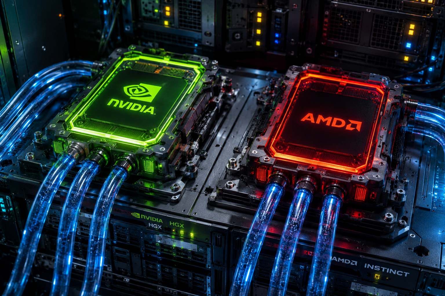
The explosive industry shift towards AI inference has ignited a fierce hardware war. Nvidia is pushing physical limits with its vertically integrated 3nm Vera Rubin platform, while AMD is aggressively countering with the memory-dense, open-standard MI400X to shatter vendor lock-in.
Why It Matters
Facing 100kW+ rack limits and soaring hardware costs, architecture dictates corporate survival. AMD’s memory advantage undercuts Nvidia on Total Cost of Ownership (TCO) for inference, forcing a multi-billion dollar diversification in global cloud infrastructure.
Executive Summary
- The Inference Shift: AI workloads have definitively transitioned from training to inference (projected at 80% by 2028), making memory density and cost-per-token the primary battlegrounds over raw compute power.
- Nvidia’s Premium Scale-Up: Nvidia’s upcoming Vera Rubin architecture pairs with 288 GB HBM4 and the proprietary CUDA/NVLink ecosystem to guarantee unparalleled Model Flops Utilization (MFU), justifying its premium pricing for complex foundational training.
- AMD’s TCO Disruption: The AMD MI400X disrupts the market with a staggering 432 GB of HBM4 and open UALink networking, significantly cutting node requirements and delivering a highly favorable Total Cost of Ownership (TCO) advantage for massive-scale inference.
- Supply & Thermal Constraints: The true limiters to 2026 AI scaling are no longer just silicon, but completely sold-out TSMC CoWoS advanced packaging, complex HBM4 supply crunches, and the mandatory, expensive transition to 100% direct-to-chip liquid cooling.
The 3nm Silicon War: Why Nvidia’s Rubin and AMD’s MI400X Are Sparking a Data Center Cold War
Inside the 2026 AI chip war: Nvidia Vera Rubin vs. AMD MI400X. We analyze HBM4 bottlenecks, liquid cooling, TCO, and enterprise cloud scaling to reveal which architecture dominates data centers.

Nvidia Next-Gen AI Architecture vs. AMD: The 2026 Battle for Enterprise Data Center Supremacy
The explosive growth of generative AI throughout 2026 has pushed global computational infrastructure to its absolute physical, economic, and thermodynamic limits. What began as an experimental race to train foundational models has rapidly matured into a massive, highly optimized industrial scale-out of inference-driven AI factories. In this hyper-accelerated landscape, the demand for Nvidia vs AMD data center GPUs has reached fever pitch, fundamentally transforming how hyperscalers, cloud providers, and Fortune 500 enterprises architect their facilities. When we look at the trajectory of the market, Nvidia, having established an iron grip on the industry, is aggressively pushing the boundaries of materials science with radically redesigned, multi-die architectures. Conversely, AMD has executed a highly strategic and aggressive comeback, leveraging memory-dense designs and an open-source software ecosystem to shatter vendor lock-in.
This next-gen AI architecture comparison will exhaustively dissect the technological and economic battlegrounds defining the semiconductor industry today. Our analysis reveals that the modern evaluation of enterprise data center AI chips goes far beyond raw theoretical compute metrics. Success in 2026 hinges on understanding the Total Cost of Ownership (TCO) for AI data centers, the complex transition to High Bandwidth Memory (HBM4), the evolving maturity of the CUDA vs ROCm ecosystem, and the critical ability to manage unprecedented AI supercomputer power consumption. By examining the upcoming hardware iterations, software ecosystems, and supply chain bottlenecks, this comprehensive report details exactly which architecture will dominate enterprise cloud deployments through the end of the decade.
The State of Enterprise AI in 2026: Market Share Dynamics and the Inference Shift
The Total Addressable Market (TAM) for AI accelerators has expanded at a staggering velocity. Growing from approximately $55 billion in 2023, the TAM reached $160 billion in 2025 and is projected to exceed $200 billion by the end of 2026. At the center of this financial vortex is Nvidia. The company’s data center revenue trajectory is historic, surging to $193.7 billion in fiscal year 2026, which represents a massive 90% of its total corporate earnings. Nvidia’s absolute dominance is anchored by an unmatched full-stack platform, proprietary software ecosystems, and prioritized allocation of global semiconductor manufacturing, allowing the company to command an estimated 80% of the merchant AI accelerator market by revenue.
However, the sheer scale of enterprise AI infrastructure investment has created an unsustainable economic dynamic for hyperscalers. Tech giants such as Microsoft, Meta, Google, and Amazon Web Services (AWS) are purchasing hundreds of thousands of GPUs annually, yet they remain deeply exposed to Nvidia’s immense pricing power, which has historically yielded 88% gross margins on flagship hardware. Enterprises needing to deploy foundational models securely can leverage managed enterprise cloud solutions via the Google Cloud Partner Network or official AWS Partner Networks . This intense economic pressure has triggered a desperate, industry-wide mandate for diversification.
Current market assessments indicate that AMD’s Instinct GPU line has capitalized on this urgency. In 2025, AMD generated an estimated $7 billion to $8 billion in data center GPU revenue, securing a critical 5% to 7% merchant market share, with 2026 projections placing them closer to 10% as capacity scales. Furthermore, the competitive landscape is no longer a simple binary. When we look at the broader ecosystem, custom silicon Application-Specific Integrated Circuits (ASICs)—such as Google’s TPUs, AWS’s Trainium and Inferentia, and Meta's MTIA—have risen dramatically. Custom silicon now represents over 20.9% of the AI chip market and is expected to expand to 27.8% by the end of 2026. Broadcom alone generated over $20 billion in AI ASIC revenue in fiscal year 2025 with an active backlog of $73 billion, while Google runs more than 75% of its Gemini workloads on internal TPUs.
The most profound structural shift dictating the 2026 market is the transition of workloads from training to inference. Inference operations—the continuous serving of deployed models—are projected to account for two-thirds of all AI compute spending this year, heading toward 80% by 2028. Inference workloads are highly price-sensitive, demand massive memory capacity, and are fundamentally less reliant on Nvidia’s proprietary software stack than foundational training workloads. This shift perfectly aligns with AMD’s hardware strategy, exposing a critical vulnerability in Nvidia’s armor and setting the stage for the most fiercely contested hardware cycle in semiconductor history.
Nvidia's Next-Gen Architecture: Pushing the Limits of Physics
To maintain its supremacy and justify its premium pricing, Nvidia has completely overhauled its engineering cadence, committing to an aggressive annual release cycle that forces competitors into a perpetual state of reaction. The transition from the Hopper and Blackwell generations into the late-2026 Rubin ecosystem represents a fundamental departure from monolithic chip designs, introducing complexities that push the very limits of materials science, packaging, and thermodynamics. While hyperscalers buy in bulk, enterprise research labs often require localized testing. Upgrading your internal hardware is a critical first step. You can check the latest pricing for custom AI-ready workstations on Dell's official store, or explore bespoke setups from Puget Systems.
Architectural Leap: From Blackwell Ultra to the Vera Rubin Platform
The immediate bridge in Nvidia’s current roadmap is the Blackwell Ultra (B300) architecture, designed for deployment across 2025 and early 2026. The B300 GPU maximizes the existing TSMC 4NP process node, delivering 15 petaFLOPS of dense FP4 compute and integrating up to 288 GB of 12-high stack HBM3e memory with 8 TB/s of bandwidth. While Blackwell Ultra represents the pinnacle of current-generation design, it is the subsequent Nvidia Rubin architecture (R100) that completely redefines the enterprise hardware landscape.
Scheduled for high-volume production and deployment in the second half of 2026, the Rubin architecture is built on the cutting-edge TSMC 3nm (N3P) process node. The R100 GPU features an astonishing 336 billion transistors distributed across a highly sophisticated multi-die chiplet design featuring two reticle-limited compute dies. This architectural leap delivers 50 petaFLOPS of FP4 inference performance per chip, a massive 5X multiplication of the capabilities seen in the baseline Blackwell generation.
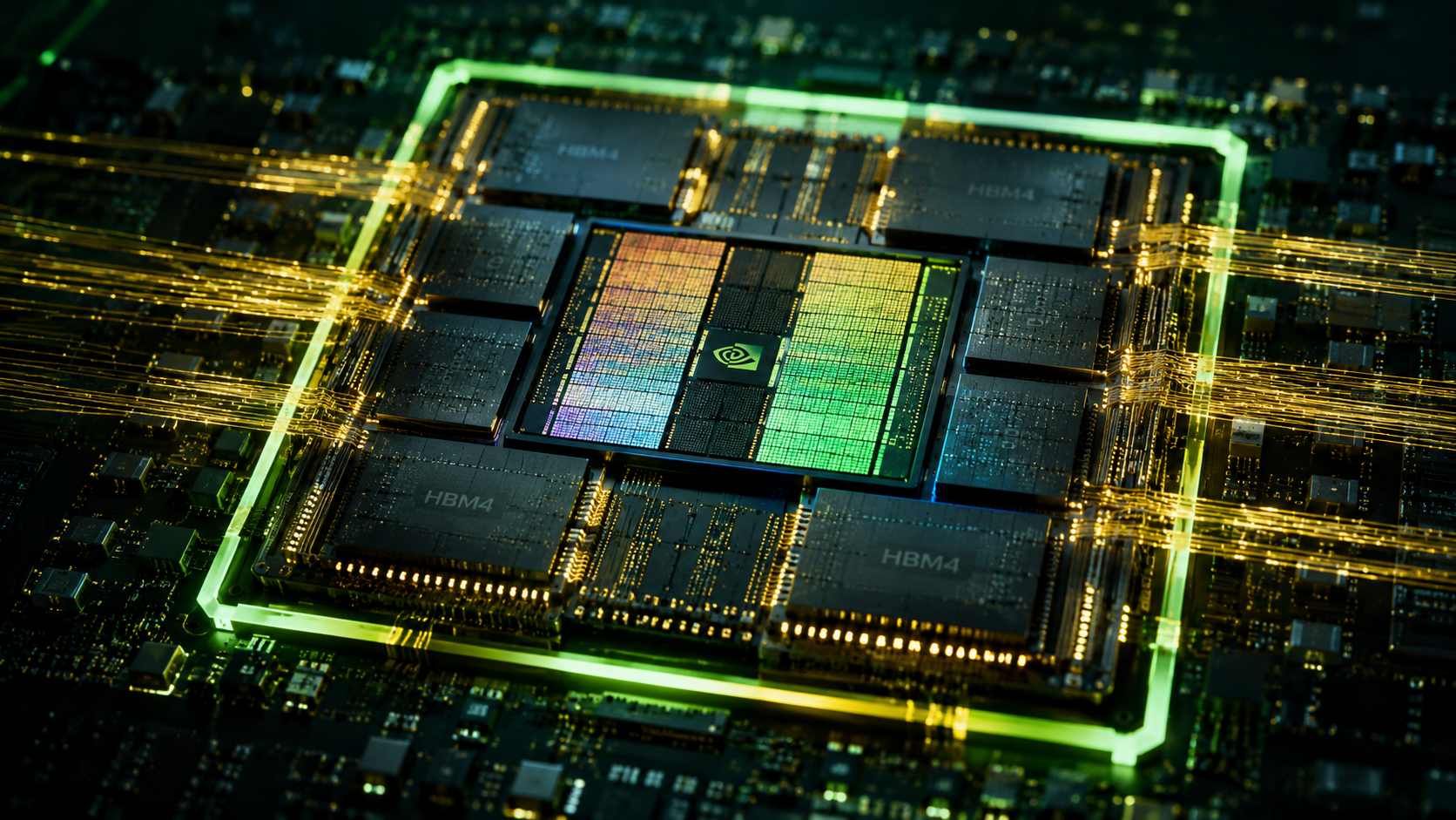
To feed this immense compute engine, Nvidia is pioneering the adoption of High Bandwidth Memory (HBM4). The Rubin GPU pairs with 288 GB of HBM4, expanding the data path with a 2048-bit interface to achieve staggering memory bandwidths reaching 22 TB/s. Furthermore, the architecture introduces a custom, highly energy-efficient ARM-based CPU known as the Vera CPU. Boasting 88 Olympus cores with spatial multi-threading (176 threads), the Vera CPU handles orchestration and agentic workloads, utilizing LPDDR5 memory to maximize rack-level power efficiency and delivering 2X the performance of the previous Grace CPU.
The ultimate expression of this architecture is the Vera Rubin NVL72 rack-scale system. Operating as a single unified supercomputer, it links 72 Rubin GPUs and 36 Vera CPUs in a completely liquid-cooled rack to deliver 3.6 exaflops of AI compute and 20.7 TB of aggregate HBM4 memory. For data center cloud hosting solutions, this translates to unparalleled throughput for processing trillions of tokens. Furthermore, Nvidia has integrated deterministic dataflow inference accelerators via Samsung-manufactured Groq LP 30 chips. Coupled tightly with the Vera Rubin platform via Dynamo software, this integration claims a massive 35x increase in throughput per megawatt compared to Blackwell.
The Power of CUDA and TensorRT: The Unyielding Software Moat
Nvidia’s absolute dominance is not purely a function of its silicon; it is deeply entrenched through the CUDA vs ROCm ecosystem dynamic. With over 5.9 million developers globally, CUDA provides an unmatched library of highly optimized primitives, compilers, and debugging tools that have become the de facto language of enterprise AI. The true bottleneck in 2026 isn't just hardware; it's the shortage of engineers who can optimize for it. Developers looking to master CUDA architecture or AMD's ROCm can upskill rapidly with expert certifications on Coursera.
The integration of TensorRT and native support for advanced frameworks like SGLang and vLLM ensures that Nvidia hardware achieves exceptionally high Model Flops Utilization (MFU). Microbenchmarks from the Hopper and Blackwell generations demonstrate that Nvidia GPUs can reliably achieve up to 93% of their theoretical peak FLOPS in real-world deployments. This efficiency is a massive economic lever; high utilization means fewer hardware purchases are required to achieve target Large Language Models (LLM) training costs.
While open-source compilers like OpenAI Triton are beginning to abstract away some of this proprietary lock-in by automatically generating optimized kernels via PTX and LLVM, Nvidia’s day-zero optimizations for new model architectures preserve a substantial performance premium in complex training environments. Our analysis highlights that for foundational model training, the software maturity of Nvidia remains a distinct, highly monetizable advantage.
Networking and Interconnects: NVLink 6 and Scale-Up Domination
As AI clusters grow to encompass hundreds of thousands of GPUs, the network effectively becomes the computer. Nvidia’s scale-up interconnect, NVLink 6, is arguably the most critical component of the Rubin architecture. NVLink 6 doubles the interconnect bandwidth of the previous generation, delivering 3.6 TB/s of all-to-all bandwidth per GPU. This allows all 72 GPUs in a Vera Rubin rack to function coherently as a single massive memory pool, completely bypassing traditional PCIe bottlenecks.
To extend this dominance and counter open-source networking threats, Nvidia introduced NVLink Fusion. This strategic initiative allows third-party CPUs from partners like Arm, Intel, and Fujitsu to connect directly into the NVLink fabric, creating semi-custom AI infrastructure. However, this "openness" comes with a strategic caveat: all connections must ultimately terminate on Nvidia's proprietary switching fabric. As industry analysts note, this creates the illusion of flexibility while reinforcing a center of gravity exclusively under Nvidia's control. Coupled with the ConnectX-9 SuperNIC (1.6 Tb/s per-GPU networking), BlueField-4 DPUs, and optical fiber interconnects targeting 200 GB/s per direction, Nvidia's networking stack ensures that large-scale training jobs are never starved for data.
AMD’s Aggressive Counter-Attack: The Instinct Series Evolution
While Nvidia focuses on building an impenetrable, vertically integrated scale-up ecosystem, AMD has positioned itself as the high-value, open-standard disruptor. By identifying memory capacity and upfront pricing as Nvidia's primary vulnerabilities, AMD’s aggressive counter-attack specifically targets the fastest-growing segment of the market: massive-scale AI inference and enterprise AI infrastructure investment.
Breaking Down the CDNA 5 Architecture: The MI400X Leap
AMD's bridge architecture, the CDNA 4-based MI350X and MI355X, successfully competes with Nvidia's Blackwell generation. Built on a 3nm process with 185 billion transistors, the MI350X matches the B200 in dense FP8 performance at ~4,600 TFLOPS while providing a substantial memory advantage with 288 GB of HBM3e. However, it is the forthcoming AMD Instinct MI400X and the broader MI400 series that serve as the true structural counterweight to Nvidia's Vera Rubin.
Scheduled for release in the second half of 2026, the AMD Instinct MI400 series will be the first GPU family manufactured on TSMC's ultra-advanced 2nm-class (N2) fabrication process. The series fractures into specialized variants to eliminate redundant execution logic and improve silicon efficiency. The MI430X is designed for sovereign AI and high-precision HPC (fully supporting FP32 and FP64), while the MI440X and MI455X are optimized specifically for low-precision (FP4, FP8, BF16) AI inference and training workloads.
The flagship Instinct MI400X accelerator is projected to deliver up to 20 PFLOPS of dense FP4 compute per package, representing a massive 10X improvement over the MI300X in handling advanced frontier models. More importantly, AMD is doubling down on its memory dominance. Each MI400X package features a staggering 432 GB of HBM4 memory across 12 stacks, achieving 19.6 TB/s of per-package bandwidth.
To deploy this advanced silicon at hyperscale, AMD introduced the Helios rack-scale architecture. Powered by next-generation Zen 6 EPYC "Venice" CPUs—which feature up to 256 high-performance cores and 1.6 TB/s of memory bandwidth—the Helios rack houses 72 Instinct MI455X accelerators. This open, OCP-compliant standard delivers 2.9 exaFLOPS of FP4 inference compute and an unprecedented 31 TB of aggregate HBM4 memory per rack, yielding an aggregate memory bandwidth of 1.4 PB/s.
The UALink Interconnect: Breaking the Proprietary Network
Recognizing that NVLink is Nvidia's strongest moat, AMD has championed the Ultra Accelerator Link (UALink) consortium. Built on IEEE 802.3 PAM4 standards, UALink is an open specification designed to deliver high performance without relying on vendor-specific silicon or proprietary cable assemblies. The UALink 1.0 specification supports up to 1,024 GPUs in a single domain with 200 GT/s bandwidth. By integrating UALink and Ultra Ethernet via upcoming Pensando Vulcano 800G network interface cards, AMD allows hyperscalers to build massive scale-out networks that prevent multi-vendor lock-in. While dedicated UALink switches are not expected until late 2026, this strategic pivot provides a clear roadmap for escaping Nvidia's networking monopoly.
The ROCm Software Ecosystem: Closing the Utilization Gap
Historically, AMD’s greatest liability has been software maturity. Microbenchmarks previously indicated that older AMD architectures struggled with clock throttling under dense tensor workloads, achieving real-world Model Flops Utilization (MFU) of only ~45%, compared to Nvidia's 50-55% at scale. With the release of AMD ROCm 7, this narrative is shifting rapidly.
ROCm 7 represents a generational leap in software optimization. It delivers up to a 3X average improvement in training workloads and an impressive 4.6X boost in inference performance over ROCm 6. By providing day-zero support for cutting-edge open-source models like LLaMA 4, Gemma 3, and DeepSeek, AMD ensures enterprises can deploy modern architectures instantly. Furthermore, ROCm 7 natively integrates with high-throughput serving frameworks like vLLM and SGLang, abstracting the hardware layer and enabling distributed inference at rack scale. Our analysis points to a significant expansion in platform support as well, with ROCm now spanning Linux and Windows and supporting endpoint devices via Ryzen AI 300 series processors and Radeon RX 7000 graphics. For enterprise data center operators, the software gap is closing, transforming the hardware decision into a pure economic calculation.
Pricing Strategy and the Memory Capacity Advantage
AMD’s penetration into the data center relies heavily on targeting the cost-conscious enterprise buyer. Upfront hardware costs for AMD systems have historically been 30% to 50% cheaper than Nvidia equivalents. Cloud pricing metrics reflect this; MI300X systems typically rent for $1.50 to $6.98 per hour, compared to $1.99 to $12.29 per hour for H100 systems.
In the realm of LLM inference, memory capacity is the absolute physical bottleneck; models must fit entirely into VRAM to be served efficiently. AMD’s strategy of providing 432 GB of HBM4 on the MI400X means that massive frontier models can be distributed across significantly fewer GPUs. Fitting a multi-hundred-billion parameter mixture-of-experts model on three AMD GPUs instead of five Nvidia GPUs results in drastic reductions in immediate capital expenditure, rack space utilization, and power draw. For B2B SaaS and data center cloud hosting solutions offering inference-as-a-service, this architectural choice translates directly into higher profit margins and lower TCO. This value proposition recently culminated in a massive 6-gigawatt data center deployment partnership between AMD and Meta, utilizing customized MI450 architecture specifically optimized for Meta's workloads.
Head-to-Head Comparison: The Battle for Total Cost of Ownership (TCO)
Evaluating enterprise data center AI chips in 2026 requires moving beyond isolated specification sheets to rigorously understand the Total Cost of Ownership (TCO) for AI data centers. TCO encompasses upfront hardware acquisition, advanced cooling infrastructure retrofits, energy consumption per token generated, and the networking required to scale to supercomputer levels. Our analysis indicates that setting up physical racks isn't always feasible for startups. If your enterprise needs instant access to scalable Nvidia or AMD GPUs for inference, you can deploy on-demand cloud infrastructure by spinning up a high-performance server on DigitalOcean, exploring Vultr's GPU instances, or starting your free trial on Cloudways.
2026 Next-Gen AI Architecture Specifications
The structural differences between Nvidia's proprietary scale-up approach and AMD's open, memory-dense strategy are most evident when analyzing rack-scale flagship solutions side-by-side.
| Specification Feature | Nvidia Next-Gen (Vera Rubin NVL72) | AMD Next-Gen (Helios Rack with MI455X) |
|---|---|---|
| Primary Target Workload | High-end Foundational Training & Agentic AI | Massive-Scale Inference & Sovereign AI |
| GPU Architecture | Rubin (R100) | CDNA 5 (Instinct MI400-Series) |
| Manufacturing Process Node | TSMC 3nm (N3P) | TSMC 2nm (N2) |
| GPU Count per Rack | 72 GPUs | 72 GPUs |
| Per-GPU Memory (HBM4) | 288 GB | 432 GB |
| Aggregate Rack Memory Capacity | 20.7 TB HBM4 | 31.0 TB HBM4 |
| Rack Compute Performance (FP4) | 3.6 ExaFLOPS | 2.9 ExaFLOPS |
| Scale-Up Interconnect | NVLink 6 (3.6 TB/s per GPU, Proprietary) | UALink & Infinity Fabric (Open Standard) |
| CPU Pairing | Vera CPU (Custom ARM, 88 Cores) | Zen 6 EPYC "Venice" (x86, up to 256 Cores) |
| Cooling Requirement | 100% Direct-to-Chip Liquid Cooled (45°C) | Direct-to-Chip Liquid Cooled |
| Strategic Advantage | Superior throughput, lowest latency scaling | Massive memory capacity, vendor flexibility |
When we look at the raw TCO numbers, the effective TCO advantage for AMD during inference workloads is highly favorable, largely due to the sheer memory density requiring fewer physical nodes. However, lower software utilization on AMD hardware partially offsets its raw price advantage during complex training workloads, leaving the effective TCO advantage for AMD closer to 15% to 25% for training.
AI Supercomputer Power Consumption and Cooling Technologies
The sheer density of these next-generation architectures has fundamentally broken traditional data center physics. AI supercomputer power consumption now dictates deployment feasibility across the globe. Both Nvidia and AMD have pushed per-rack power consumption far beyond the 40 kW limits of older air-cooled facilities, routinely designing loads that exceed 100 kW to 120 kW per rack, with flagship individual GPUs reaching thermal design powers (TDP) estimated at 1400W to 1600W.
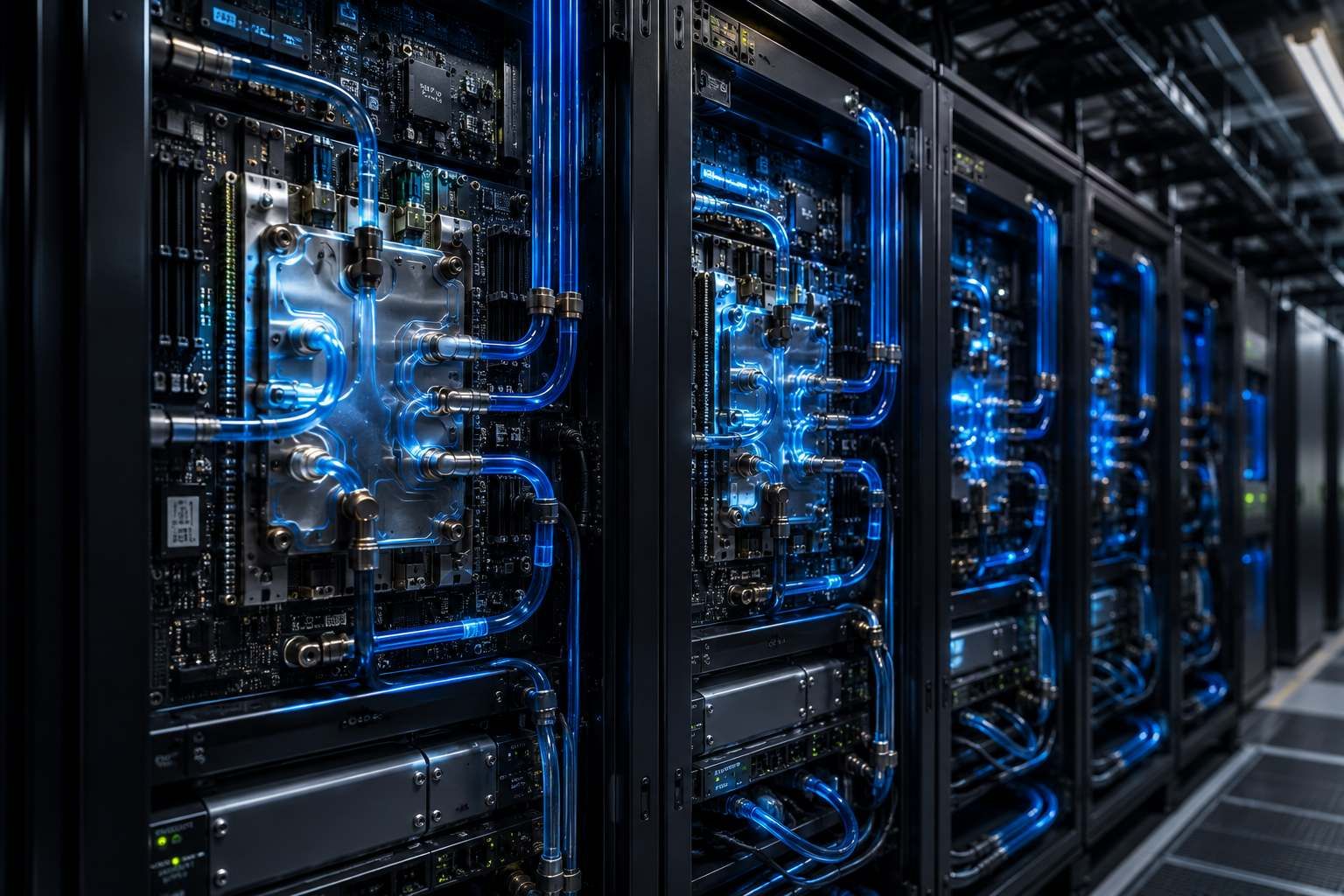
Consequently, liquid cooling is no longer a localized optimization; it is a mandatory facility requirement. Nvidia’s Rubin architecture is strictly 100% liquid-cooled, explicitly engineered to run on 45°C hot water. Traditional air-cooled infrastructure is entirely insufficient. Goldman Sachs projects the share of liquid-cooled AI servers will climb from 15 percent in 2024 to 76 percent in 2026.
This requires the extensive deployment of specialized server rack cooling technologies, primarily Direct-to-Chip (DTC) cooling plates and highly advanced Coolant Distribution Units (CDUs). The CDU market is experiencing explosive growth, valued at over $1.8 billion in 2026, with Rack-Level CDUs dominating (41% market share) due to the need for localized, high-efficiency cooling in high-density environments. Direct-to-Chip cooling commands a 56% market share as it efficiently manages extreme heat loads.
Companies like Trane Technologies and LG Electronics have aggressively expanded their enterprise offerings, delivering megawatt-scale CDUs that combine inverter-driven pumps and integrated software to orchestrate thermal management. These CDUs manage the separation of primary facility-level water loops from the secondary coolant loops directly touching the silicon via plate heat exchangers, enabling optimal thermal transfer without the risk of catastrophic facility contamination. This transition forces data center cloud hosting solutions to incur massive brownfield retrofit costs. However, architectures like Vera Rubin can deliver up to 35x more token throughput per megawatt compared to older generations. Therefore, while the upfront power infrastructure investment is staggering, the unprecedented energy efficiency measured in "tokens per watt" highly incentivizes the transition to these next-generation nodes.
The TSMC Bottleneck and Geopolitical Supply Chain
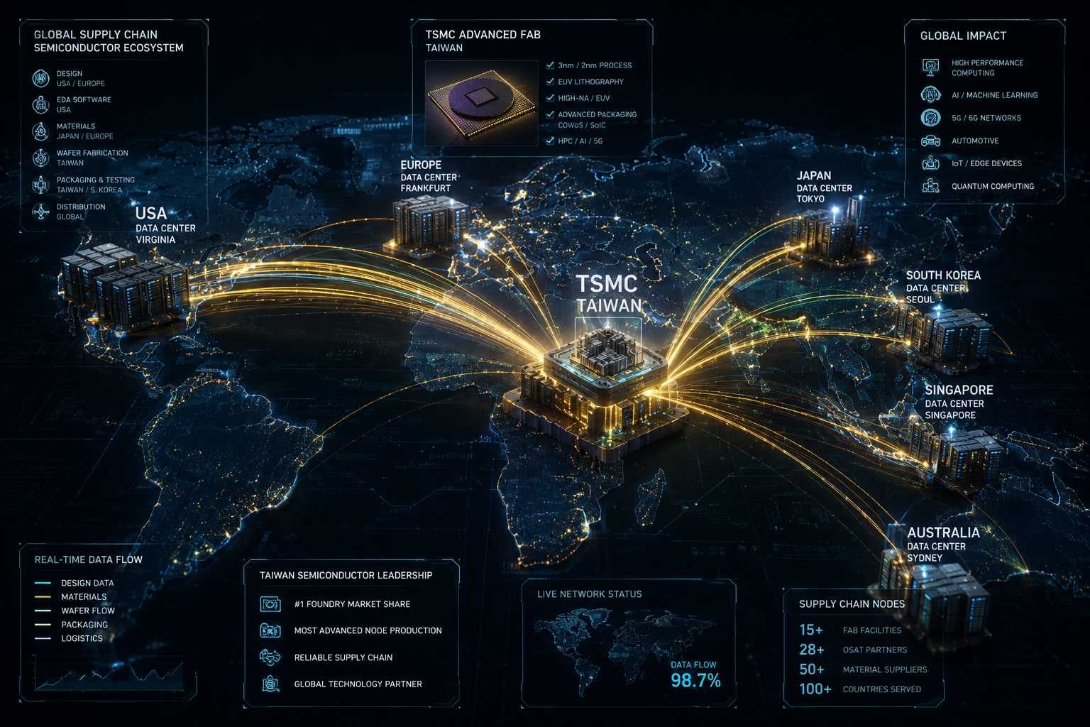
No degree of architectural brilliance can overcome the physical constraints of the AI hardware supply chain. Both Nvidia and AMD are entirely reliant on Taiwan Semiconductor Manufacturing Company (TSMC) to fabricate their silicon, creating profound supply bottlenecks that directly impact enterprise delivery schedules and trigger immense interest from Wall Street investors. When we look at the supply chain bottlenecks, semiconductor stocks remain highly volatile. Investors looking to capitalize on this AI hardware supercycle can track and trade NVDA or AMD options using trade tech stocks directly on platforms like [open a trading account on Robinhood] or [start trading options on Webull].
Advanced Node and CoWoS Packaging Shortages
The transition to TSMC 2nm and 3nm node manufacturing requires intense capital commitment. Capacity for these cutting-edge nodes is severely constrained. For teams planning tape-outs, 2nm capacity is essentially fully booked through 2027 at fabs like Fab 20 and 22, while N3/N4 processes require 12+ months of advance commitment, pushing lead times to 39–78 weeks.
However, our analysis indicates that the true epicenter of the 2026 supply chain crisis is not the silicon wafer itself, but advanced packaging. TSMC’s CoWoS (Chip-on-Wafer-on-Substrate) technology is mandatory for assembling multi-die AI accelerators and attaching high-bandwidth memory. Despite TSMC aggressively scaling CoWoS production from approximately 35,000 wafers per month in late 2024 to a projected 130,000 wafers per month by the end of 2026—a nearly 4x increase—the technology remains completely sold out. Nvidia has historically reserved the vast majority of CoWoS allocations due to its massive volume guarantees, which leaves competitors scrambling to secure enough backend packaging capacity to turn their fabricated dies into functional products.
The HBM4 Manufacturing Complex
The industry-wide adoption of High Bandwidth Memory (HBM4) introduces a secondary, highly volatile bottleneck. Unlike previous memory standards like HBM3e where the DRAM supplier handled almost all manufacturing independently, HBM4 requires a complex joint-manufacturing model. The memory manufacturer must build taller, denser 12 to 16 high-interface DRAM layers on top of a logic base die typically fabricated by a foundry partner.
This deep integration dramatically increases the complexity of bonding steps, inherently capping initial yields and creating an intense supply crunch. Samsung, vertically integrated, is combining its 1c DRAM process with its own 4nm foundry logic base die, aiming to challenge the current market leaders. Meanwhile, SK Hynix, which led the global HBM market with a 57% share, relies on TSMC's 12nm and 3nm processes for base die production.
Nvidia’s insistence on driving HBM4 pin-speeds far beyond initial JEDEC industry standards (pushing targets from 9.6 Gbps to exceeding 11 Gbps to 13 Gbps) forced mid-cycle redesigns across the "HBM Trio"—SK Hynix, Samsung, and Micron. With global HBM4 capacity fully allocated and pledged to major hyperscaler programs (like Nvidia's Rubin and Google's TPU), memory has become a strategic weapon. For enterprise IT decision-makers, tracking TSMC CoWoS capacity and SK Hynix yield rates is just as critical as analyzing hardware benchmarks, as supply chain availability will ultimately dictate deployment realities.
Which Architecture Should Enterprise Cloud Providers Choose?
Enterprise IT decision-makers and cloud hosting architects at tier-one providers like AWS, Azure, and Google Cloud are no longer standardizing on a single hardware vendor. The extreme financial stakes require a bifurcated infrastructure strategy tailored to specific workloads.
For Supreme Performance and Software Maturity: Nvidia Remains the King When the primary objective involves training massive trillion-parameter foundational models or operating highly complex, latency-sensitive agentic AI frameworks, Nvidia’s architecture remains unparalleled. The Vera Rubin NVL72 rack, backed by the 3.6 TB/s all-to-all bandwidth of NVLink 6 and the deep, day-zero optimizations of the CUDA ecosystem, guarantees the highest Model Flops Utilization (MFU). For cloud providers catering to tier-one AI research labs where time-to-market is the only metric that matters, paying the Nvidia premium is an operational necessity. Azure's early integration of Rubin racks into their Fairwater AI superfactories exemplifies this commitment to absolute peak performance. Similarly, AWS is aggressively expanding its capacity, committing to deploying over 1 million Nvidia GPUs, including Blackwell and Rubin architectures, starting in 2026.
For Raw Compute per Dollar and Memory Capacity: AMD is the Disruptive Alternative Conversely, the economics of AI are rapidly shifting toward widespread, global inference. For B2B SaaS platforms running massive enterprise databases, sovereign AI deployments, or generative AI applications serving millions of daily queries, the memory-dense AMD Instinct MI400X offers a superior Return on Investment. The provision of 432 GB of HBM4 per GPU fundamentally lowers Large Language Models (LLM) training costs and inference serving costs by drastically reducing the number of physical nodes required to host a model. Furthermore, AMD's reliance on open interconnects like UALink and its integration with the open-source ROCm 7 ecosystem prevents hyperscalers from being permanently locked into proprietary networking fabrics. This makes AMD the hardware of choice for cost-effective, highly scalable cloud deployment, a thesis validated by Meta's monumental 6-gigawatt infrastructure deal powered by AMD hardware.
FAQs
Which is better for training LLMs, Nvidia or AMD? For foundational training of advanced frontier models from scratch, Nvidia currently maintains an advantage due to the deep optimizations of the CUDA ecosystem, higher Model Flops Utilization (MFU), and the superior scale-up bandwidth of NVLink. However, AMD is rapidly closing the gap with its ROCm 7 updates and the introduction of the MI400X, making it highly competitive for fine-tuning and massive-scale inference workloads.
Will AMD ever beat Nvidia in the data center market? While AMD is unlikely to dethrone Nvidia's total revenue dominance in the near term, it has successfully established itself as a critical counterweight. By focusing on memory capacity and open-source flexibility, AMD is projected to capture highly lucrative segments of the inference market, pushing its market share into double digits and forcing Nvidia to compete on pricing and open standards. Custom ASICs also represent a growing threat to Nvidia's market share.
What is the power consumption of next-gen AI GPUs? Next-generation AI architecture requires unprecedented power, with rack-scale configurations pushing past 100 kW to 120 kW per rack. Flagship individual GPUs like the upcoming MI400X and Blackwell Ultra are estimated to reach thermal design powers (TDP) exceeding 1400W to 1600W. This extreme density mandates the use of 100% direct-to-chip liquid cooling and advanced Coolant Distribution Units (CDUs) to maintain safe operating temperatures.
Conclusion
The 2026 battle for enterprise data center supremacy is a clash of fundamentally different philosophies. Nvidia’s strategy revolves around the Vera Rubin architecture—a highly proprietary, vertically integrated ecosystem that leverages extreme interconnect speeds and the entrenched CUDA software moat to deliver absolute peak performance. In stark contrast, AMD’s aggressive counter-attack relies on the CDNA 5 architecture, the memory-dense MI400X, and the open-source ROCm platform to commoditize the hardware layer and offer cost-effective, high-capacity inference solutions. Ultimately, as the enterprise focus shifts aggressively toward running large language models in production, success will be dictated not just by pure teraflops, but by mastering the Total Cost of Ownership, securing TSMC advanced packaging, and deploying highly efficient liquid cooling infrastructure.
Which hardware strategy aligns with your 2026 infrastructure roadmap? Are you bullish on Nvidia's proprietary performance, or investing in AMD's disruptive, memory-dense enterprise solutions? Investors can follow the latest hardware Investors can follow the latest hardware trends and open a trading account directly on platforms like Robinhood, or start trading options on Webull.
Disclosure: This article may contain affiliate links. If you purchase or sign up through these links, we may earn a small commission at no extra cost to you. This helps support our editorial team.
Unlock the full Institutional Analysis
This is a premium deep-dive report. Join an elite community of investors, CEOs, and analysts who receive our exclusive global intelligence for free.
No spam. Unsubscribe anytime.
Related Topics:
"Tracking the carbon economy, decoding global climate treaties, and analyzing the massive environmental forces reshaping human civilization and global industry."
"Decoding the rapid evolution of artificial intelligence, deep-space breakthroughs, and the critical frontier of human science and bio-tech."
"Decoding the rapid evolution of artificial intelligence, deep-space breakthroughs, and the critical frontier of human science and bio-tech."
"Decoding the high-stakes chess game of global statecraft, strategic diplomacy, and the shifting balance of world power."
"Curating the elite intersection of global culture, cinematic intelligence, high-end gastronomy, and the premium evolution of modern lifestyle."

WPP Frontier Labs
Decoding the rapid evolution of artificial intelligence, deep-space breakthroughs, and the critical frontier of human science and bio-tech.
Get the Weekend Intelligence Briefing
Sign up for the deepest geopolitical and tech insights sent directly to your inbox every Sunday.
No spam. Unsubscribe anytime. View our Privacy Policy.