Smart Reading Mode Enabled
Double-click or long-press any difficult word in this article to instantly view its definition.
Semiconductor Market Forecast: AI Chip Stocks & US CHIPS Act Impact
Explore the 2026 global semiconductor supply chain forecast. Discover how AI chip demand, HBM4 memory, and the US CHIPS Act are shaping top semiconductor stocks through 2030.


Global Semiconductor Supply Chain Analysis 2026: Navigating Geopolitical Realignment, Next-Gen AI Silicon, and the Trillion-Dollar Market Threshold
The Structural Transformation of the Silicon Ecosystem
When we look at the current landscape, it is clear that the global semiconductor industry has decisively entered the most critical, highly complex, and economically consequential phase of its historical development. As of 2026, we can see that the sector is no longer defined by the frictionless globalization and highly integrated, cross-border networks that characterized the previous two decades. Instead, our analysis reveals that the ecosystem is undergoing a violent structural realignment. A comprehensive Global Semiconductor Supply Chain Analysis 2026 shows us that the industry is actively fragmenting into competing regional spheres of influence, driven by an intense convergence of geopolitical friction, aggressive state-sponsored industrial policies, and the explosive, insatiable computational demands of generative artificial intelligence (AI).
In our view, control over advanced semiconductor manufacturing has become synonymous with global hegemonic power and national security. This reality has prompted national governments across the United States, the United Kingdom, the European Union, and East Asia to aggressively pursue "chip sovereignty" through the heavy subsidization of domestic fabrication capabilities and the implementation of stringent export controls. Simultaneously, we are observing that the technological paradigms that govern the industry are being pushed to the absolute boundaries of physics. The Future of Semiconductor Manufacturing is forcing a rapid pivot away from traditional transistor scaling toward highly complex advanced packaging, gate-all-around architectures, extreme ultraviolet lithography, and silicon photonics.
For the institutional investors, corporate supply chain architects, and policymakers navigating the high-stakes US and UK markets, our analysis suggests that understanding the Semiconductor Market Forecast 2026-2030 requires an extraordinarily multi-dimensional analytical framework. When we look at financial valuations, capital expenditure roadmaps, and the trajectories of Next-Gen AI Chips and Semiconductor Stocks, they are increasingly dictated not solely by architectural superiority, but by a company's access to constrained physical resources, its immunity to sovereign export controls, and its ability to navigate a profoundly distorted pricing environment characterized by unprecedented structural inflation. We are witnessing the industry rapidly bifurcating into a high-margin, AI-driven vanguard that captures nearly all economic profit, and a stagnant, commoditized legacy sector fighting for survival, fundamentally altering the risk-reward calculus for global stakeholders.
Global Semiconductor Supply Chain Analysis 2026: Geopolitical Fragmentation and Strategic Reshoring
The historically integrated semiconductor ecosystem—which relied on incredibly complex, highly efficient networks spanning the United States, Taiwan, South Korea, Japan, and the European Union—has severely deteriorated in both transparency and predictability. In our experience, the pursuit of maximum supply chain efficiency and just-in-time inventory management has been permanently replaced by the pursuit of national security and systemic resilience.
The United States Strategy: CHIPS Act Maturation, Tariff Escalations, and Export Controls

When we examine the United States, we see a nation that has catalyzed this global regionalization through an aggressive combination of massive domestic manufacturing subsidies and highly restrictive export controls. Building upon the foundational investments of the 2022 CHIPS and Science Act, our analysis points to 2026 as the critical execution phase where multi-billion-dollar federal allocations begin materializing into physical, operational capacity. Notably, the $6.6 billion in direct funding and an additional $5 billion in low-cost loans awarded to Taiwan Semiconductor Manufacturing Company (TSMC) to construct advanced logic fabrication plants in Phoenix, Arizona, illustrates the absolute strategic imperative of reshoring leading-edge production. In our latest review of the data, we can also see that in May 2026, the Department of Commerce took further steps by announcing letters of intent for $2.013 billion in federal incentives to accelerate U.S. leadership in Quantum Computing, alongside an additional $277 million for USA Rare Earth to support a domestic "mine-to-magnet" strategy.
While TSMC leadership publicly maintains that these massive capital deployments are driven by underlying customer demand and a desire to circumvent elevated import tariffs, we believe the geopolitical subtext is unavoidable. Taiwan's domestic political discourse has heavily debated the potential weakening of its "silicon shield"—the widely held strategic concept that Taiwan's indispensable monopoly over advanced semiconductor manufacturing deters Chinese military aggression by making the island too economically vital to the global economy to risk destroying.
However, we must note that domestic reshoring alone does not entirely insulate the US market from volatility. Elevated tariffs and tightening export controls actively distort the total cost of ownership for all semiconductor components. Trade escalations heading into 2026 have prompted supply chain models to project potential tariff increases of 15% to 25% on semiconductor imports from primary East Asian manufacturing hubs. These tariff increases directly erode gross margins for downstream technology manufacturers, necessitating aggressive pricing renegotiations and altering consumer pricing strategies.
Furthermore, we've observed that stringent export restrictions on advanced semiconductors have introduced substantial licensing barriers into the procurement process. These regulatory frictions pose a severe threat of causing inbound shipment delays, typically modeled at three to four weeks for North American and European integrators. This delay directly impacts manufacturing capacity, raises inventory holding costs, and hinders the achievement of service-level agreements. When we look at the most profound and immediate impact of US geopolitical policy, it is observed in the artificial constriction of the Chinese market. Semiconductor companies that once relied heavily on Chinese data-center revenue have seen those lucrative revenue streams effectively zeroed out by federal decree. Nvidia’s fiscal first-quarter reporting confirmed absolutely zero China data-center compute revenue—a market that previously accounted for at least a fifth of its highly profitable segment—due to stringent US bans on chips such as the H20 and other advanced AI accelerators.
The United Kingdom Semiconductor Strategy: Niche Optimization, IP Protection, and Capacity Deficits
In stark contrast to the massive, highly capital-intensive fabrication construction programs seen in the United States and the European Union, our analysis of the United Kingdom National Semiconductor Strategy shows a highly targeted, intellectually focused approach that matches its specific economic scale and historical strengths. Committing roughly £1 billion over a decade—a relatively modest sum compared to global equivalents—the UK strategy explicitly avoids the delusion of attempting to build mass state-of-the-art silicon fabrication plants to compete with global giants. Instead, we see the UK leveraging its rich heritage in advanced academic research to dominate specific, highly lucrative niches within the broader supply chain.
The core pillars of the UK strategy center on world-class chip design and intellectual property (IP) generation, compound semiconductors, and hardware-level security. Compound semiconductors, which utilize materials beyond traditional silicon, are absolutely essential for high-efficiency power electronics, electric vehicle grids, and advanced radar systems. Furthermore, a critical component of the UK's geopolitical strategy that we track is the commercialization of the Digital Security by Design (DSbD) initiative and the Capability Hardware Enhanced RISC Instructions (CHERI) architecture. By embedding security protocols directly into the processor's fundamental instruction set, the UK aims to eliminate entire classes of devastating memory vulnerabilities, such as buffer overflows, positioning British IP as an indispensable, non-replicable component of global critical infrastructure networks. To foster this innovation, the UK is aggressively funding specialized research hubs, including the Centre for Heterogeneous Integration of MicroElectronic and Semiconductor Systems (CHIMES) and the Compound Semiconductor Manufacturing Hub, to master the complex art of advanced packaging.
Despite these undeniable advanced research capabilities, it is our observation that the United Kingdom faces severe, systemic industrial capacity hurdles. The national strategy has been heavily critiqued by industry experts for lacking the relentless momentum and financial firepower required to translate academic prowess into tangible industrial resilience. The glaring absence of a domestic mainstream fabrication facility focused on immersion deep-ultraviolet (DUV) lithography—specifically capable of producing critical chips at the 65 nm to 28 nm scale—leaves the nation's automotive manufacturing, defense contracting, and national power grid sectors perilously exposed to international supply shocks. Without a secure domestic baseline of trailing-edge manufacturing, the UK's advanced packaging researchers lack the physical silicon required to construct the complex, multi-chip heterogenous devices they conceptualize, potentially forcing them to rely on the very volatile foreign supply chains the strategy aims to mitigate.
Strategic Imperatives for Corporate Supply Chain Architects
Based on our analysis, the violent convergence of these geopolitical variables demands a total, uncompromising overhaul of corporate procurement strategies. Legacy supply chain systems reliant on static supplier relationships, historical demand forecasting, and cost-first optimization are critically obsolete in 2026. Real-time supply chain visibility and predictive intelligence have transitioned from optional competitive advantages into absolute operational necessities.
We strongly advise that supply chain professionals must establish comprehensive, AI-driven control towers that seamlessly integrate data from enterprise resource planning (ERP) systems, global logistics tracking networks, and supplier portals to enable end-to-end transparency from the fabrication facility down to final assembly. Crucially, enterprises must move beyond simple geographic supplier diversification and engage in active, highly sophisticated geopolitical scenario planning. This involves modeling severe, high-impact disruptive events. For instance, our models show that architects must simulate a hypothetical four-to-six-week facility disruption affecting 20% to 30% of global semiconductor capacity heavily localized in Taiwan. Running these simulations allows organizations to stress-test alternative sourcing pathways, calculate optimal safety stock buffers, and evaluate the impact on customer fulfillment before a crisis occurs. Ultimately, we believe supply chain organizations are increasingly required to accept a structurally higher total cost of ownership in exchange for the redundancy and systemic resilience required to survive the next decade of semiconductor fragmentation.

Semiconductor Market Forecast 2026-2030: Memflation, The Trillion-Dollar Threshold, and the Silicon Squeeze
When we evaluate the financial trajectory of the global semiconductor industry, it reflects an environment of extreme, highly concentrated growth offset by severe structural inflation and a violently bifurcated demand landscape. By the end of 2026, our analysis indicates the global semiconductor market will cross historic financial thresholds, driven almost entirely by the relentless expansion of AI infrastructure and the compounding costs of raw materials and complex manufacturing processes.
The 2026 Revenue Surge and the Destructive Mechanics of "Memflation"
Our industry projections establish 2026 as a year of unprecedented, record-breaking financial expansion. Worldwide semiconductor revenue is forecasted to surge by an astonishing 64% exceeding the $1.3 trillion threshold to reach an estimated $1,320.2 billion. This marks the industry's third consecutive year of double-digit percentage growth, a velocity unseen in the last two decades of market tracking. However, when we look deeper at the composition of this revenue, it reveals deep underlying market distortions that threaten broader economic stability.
A primary catalyst for the massive 2026 revenue spike is the phenomenon we term "memflation"—extreme, structural price inflation across the global memory tier. Memory revenue is expected to nearly triple in a single year, skyrocketing from $216.3 billion in 2025 to an estimated $633.3 billion in 2026. This surge is engineered by a massive, deliberate supply-demand imbalance. As top-tier memory fabricators aggressively pivot their highly constrained cleanroom capacities toward producing high-margin High-Bandwidth Memory (HBM) strictly required for AI accelerators, the supply of traditional standard DDR DRAM and NAND flash utilized in standard computing is artificially choked.
Consequently, 2026 forecasts indicate absolutely staggering annual price increases of 125% for standard DRAM and an unprecedented 234% for NAND flash memory. We note that this memflation carries highly destructive second-order effects for the broader technology ecosystem. Elevated memory costs are actively destroying or severely delaying non-AI computing demand, as enterprise IT budgets and consumer electronics manufacturers simply cannot absorb the margin compression required to build standard servers, laptops, and smartphones. Financial analysts project that meaningful pricing relief in the memory sector will not materialize until late 2027 at the earliest. Consequently, our advice to Chief Information Officers (CIOs) and enterprise IT leaders is to exercise extreme caution and reject long-term supply agreements containing unfavorable pricing parameters extending beyond that date.
| Market Segment Revenue | 2025 Projected (Billions USD) | 2026 Projected (Billions USD) | 2027 Projected (Billions USD) |
|---|---|---|---|
| Global Memory Sector | 216.3 | 633.3 | 748.1 |
| Global Nonmemory Sector | 589.0 | 686.9 | 806.4 |
| Total Worldwide Market | 805.3 | 1,320.2 | 1,554.5 |
Data reflecting the disproportionate impact of memory inflation and AI infrastructure on total semiconductor revenues.
The 2030 Horizon: The Trillion-Dollar Baseline and the Extinction-Level "Silicon Squeeze"
Looking toward the end of the decade, our analysis indicates the industry is projected to firmly establish itself well above the trillion-dollar mark. In fact, comprehensive industry modeling now projects the global semiconductor market will reach $1.6 trillion by the end of 2030, climbing at a compound annual growth rate of 13%. Within this massive macro-expansion, data center semiconductors alone are forecast to account for $843.2 billion by 2030, absorbing nearly half of the entire global silicon output. We can see that the industry has crossed a fundamental structural threshold; AI is no longer categorized as a mere demand catalyst or cyclical trend. It has become the foundational base upon which all modern semiconductor capital expenditure is built.
However, we must warn that this massive aggregate wealth generation masks a highly alarming, potentially extinction-level structural crisis for legacy players termed the "Silicon Squeeze." The semiconductor industry has bifurcated into a brutal "tale of two industries". The economic profit of the entire sector is ruthlessly concentrated at the very top of the value chain. Our data indicates that the top 5% of semiconductor firms—an elite oligopoly including apex hyperscaler GPU suppliers, advanced logic foundries, and lithography monopolists—capture literally all of the industry's economic profit, generating well over $147 billion annually.
Conversely, when we look at the middle 90% of semiconductor companies, they are facing a terrifying reality of stagnant growth and persistent, highly elevated inventory levels. For this vast majority, average economic value generation has plummeted below pre-pandemic levels to roughly $17 million per company. Even more concerning, the bottom 5% of the industry is actively destroying massive amounts of capital, generating aggregate losses in the tens of billions of dollars. For companies lacking direct exposure to AI workloads or the rapidly maturing Mainland Chinese domestic market, the forecasted CAGR through 2030 collapses to a mere 2% to 3%, representing less than a third of the sector's historical historical growth rate.
To survive this violent squeeze, we believe legacy semiconductor firms must urgently transition their product portfolios, reinvent traditional business models via aggressive vertical integration, and rapidly adopt internal generative AI tools to accelerate product development, counteract a rapidly aging workforce, and fill the emerging global engineering talent void.
Segmental Demand Drivers: Computing, Wireless, and Automotive Dominance
The estimated $825 billion of absolute total market growth expected between 2024 and 2030 will not be distributed evenly. Based on our analysis, it will be highly concentrated across three dominant industry verticals :
- Computing and Data Storage: We project this vertical to experience explosive growth, surging from $350 billion in 2024 to an astonishing $810 billion by 2030, representing well over half of the total expected market expansion. This is heavily fueled by endless demand for AI training and inference servers, the incredibly high material cost of HBM (which is growing at a 20%CAGR), and the consistently rising wafer average selling prices (ASPs) commanded by advanced leading-edge nodes shrinking below 3 nanometers.
- Wireless Communications: When we look at the wireless segment, it is forecasted to expand by $150 billion, reaching a total value of $350 billion by 2030. Growth drivers include the continuous global transition to advanced 5G and early 6G connectivity standards, the migration to smaller node sizes in mobile system-on-chips (SoCs) to preserve battery life, and consumer demographics rotating into higher-tier hardware models that inherently require greater silicon density and sophisticated RF components.
- Automotive Electronics: The automotive segment represents a massive, highly durable growth driver for both advanced and mature semiconductor nodes. The accelerating proliferation of electric vehicles (EVs) is generating explosive demand for specialized power electronics, which are projected to grow at a blistering 23%CAGR. Concurrently, the architectural centralization of electronic control units (ECUs) and the ubiquitous deployment of advanced driver-assistance systems (ADAS) are consuming unprecedented volumes of data-processing accelerator chips and sensor arrays.
| Core Semiconductor Vertical | Estimated Value 2024 (Billions USD) | Projected Value 2030 (Billions USD) | Primary Growth Drivers |
|---|---|---|---|
| Computing & Data Storage | 350 | 810 | AI Servers, HBM ($20\%$ CAGR), Leading-Edge ASPs |
| Wireless | 200 | 350 | 5G/6G Transition, Complex SoCs, High-Tier Device Demand |
| Automotive | 75 | Significant Growth | EV Power Electronics ($23\%$ CAGR), ADAS, Centralized ECUs |
Segmental value projections highlighting the massive capital shift toward high-performance computing and automotive electrification.
The Future of Semiconductor Manufacturing: Breaking the Angstrom Barrier and Advanced Packaging

As the traditional tenets of Moore's Law face seemingly insurmountable physical and economic barriers, we are seeing the Future of Semiconductor Manufacturing being radically rewritten. The roadmap through 2026 and extending into the 2030s is defined not merely by shrinking transistors, but by exotic architectural geometries, the deployment of next-generation optical photolithography, and the absolute necessity of integrating multiple chips via advanced 3D packaging.
The Angstrom Era: Gate-All-Around (GAA) and the High-NA EUV Monopoly
Our analysis shows that the transition into sub-2nm "Angstrom" nodes requires a complete architectural overhaul of the fundamental logic transistor. To combat severe quantum tunneling and current leakage at microscopic scales, the industry is actively migrating away from traditional FinFET geometries to Gate-All-Around (GAA) nanosheet transistors. GAA architecture allows the conductive gate to contact the silicon channel on all four sides, drastically reducing power leakage and delivering the superior computational power and extreme energy efficiency absolutely essential for the thermal constraints of modern AI data centers. For non-memory leading-edge nodes, the demand trajectory is staggering. The 2 nm node class is expected to witness a massive 136%demand increase through 2030, while future ultra-advanced 1.4 nm nodes exhibit a projected CAGR exceeding 314%.
Executing these nanoscale dimensions requires the immediate commercial deployment of High-Numerical Aperture (High-NA) Extreme Ultraviolet lithography. ASML, the undisputed global monopolist in this highly specialized domain, announced in mid-2026 that the very first commercial chips manufactured using High-NA EUV would reach the consumer market within months, marking a monumental milestone in materials science. High-NA systems feature incredibly advanced precision optics developed in exclusive partnership with Carl Zeiss, enabling the printing of significantly smaller features without resorting to expensive, time-consuming, and error-prone multi-patterning techniques. However, we must highlight that the astronomical capital expenditure required to procure, install, and operate High-NA EUV infrastructure—running into hundreds of millions of dollars per single machine—guarantees massive structural industry consolidation. Only an elite, highly capitalized oligopoly of foundries possesses the balance sheet necessary to compete at this bleeding edge.
Intel's Foundry Turnaround: The 18A Node, Apple Partnerships, and the 14A Horizon
When we evaluate the global manufacturing landscape in 2026, Intel’s incredibly high-stakes, capital-intensive pivot to restore its former foundry dominance is central. Recognizing the national security implications of an Asia-dominated supply chain, Intel has committed over $100 billion to expand its geographic manufacturing footprint, anchored by massive new fabrication complexes in Arizona, Ohio, and Europe, to establish a viable Western alternative to TSMC and Samsung. The absolute linchpin of this turnaround strategy is the execution of the Intel 18A process node.
Intel 18A is a highly ambitious manufacturing node that simultaneously introduces two monumental structural upgrades to the silicon: RibbonFET (Intel's proprietary implementation of GAA transistors) and PowerVia (a revolutionary backside power delivery network technology). By relocating the entire power routing network to the backside of the silicon wafer, PowerVia eliminates signal routing congestion on the front side, resulting in massive density improvements and highly significant clock-speed advantages. Heading into the latter half of 2026, Intel CEO Lip-Bu Tan reported highly encouraging, verifiable metrics, noting that 18A manufacturing yields were steadily improving by an impressive 7% to 8% every single month. Furthermore, CFO David Zinsner officially confirmed that the 18A node is progressing significantly ahead of internal schedules, poised to hit final yield targets by mid-2026 rather than the original year-end projection.
This technical momentum is translating into crucial, highly visible commercial validation. The 18A-powered "Panther Lake" client CPUs have already accumulated over 200 distinct design wins, pushing Intel to aggressively pressure PC original equipment manufacturers (OEMs) to transition away from older, less efficient Intel 7 architectures. More importantly for the viability of the external foundry business, Intel recently secured a preliminary chip-making agreement with Apple to leverage the 18A node for future devices. We view this agreement as a monumental vote of confidence that provides vital, external proof of concept to hesitant fabless designers who previously doubted Intel's ability to act as an independent contract manufacturer. Looking even further ahead to maintain the pressure, Intel is already distributing the 0.5 Process Development Kit (PDK) for its upcoming 14A node to external customers, with risk production strictly aligned for 2028 and high-volume production slated for 2029, a timeline strategically aimed at directly intercepting TSMC's advanced A14 schedule.
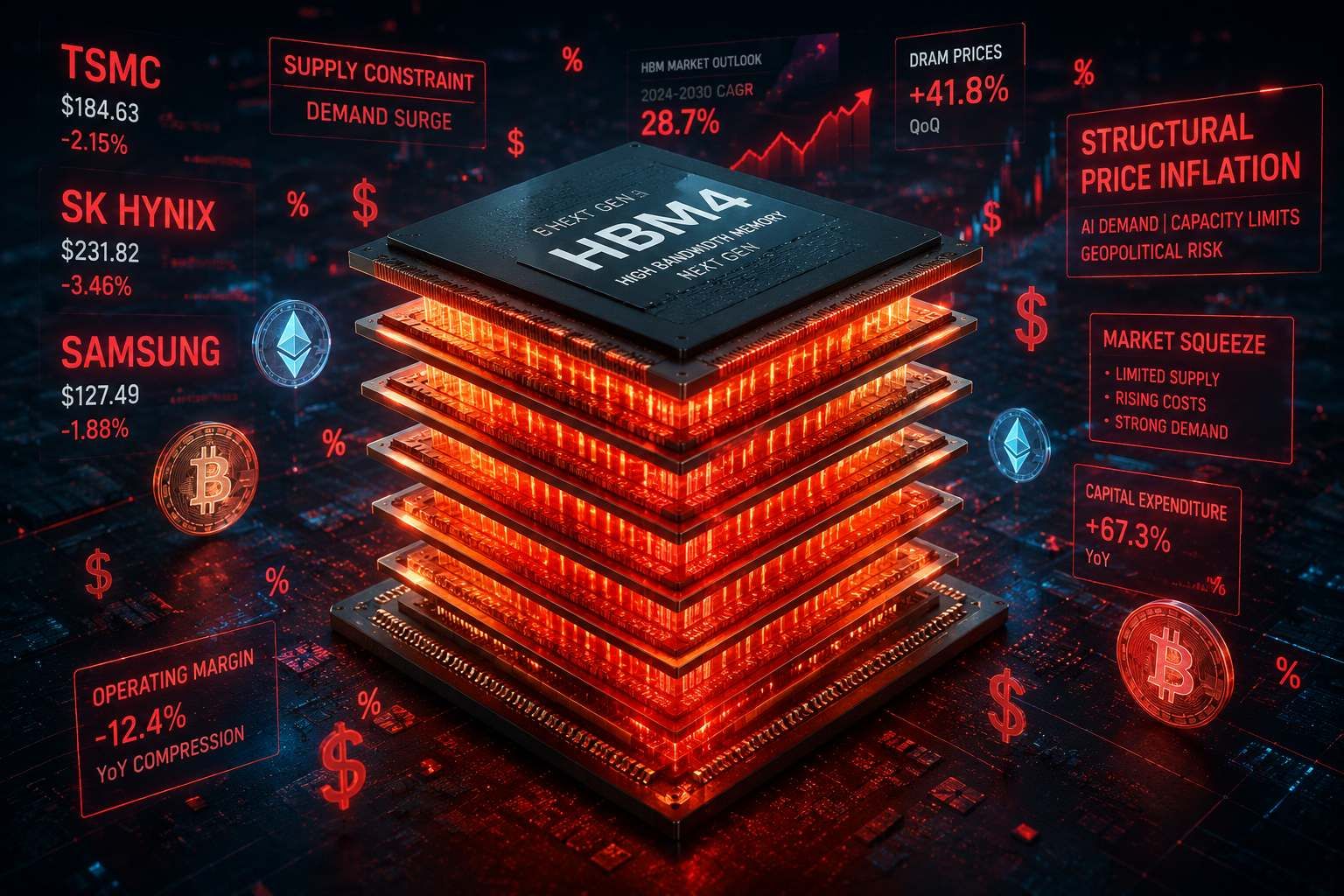
Advanced Packaging and the HBM4 Supercycle
Because shrinking massive, monolithic silicon dies is becoming prohibitively expensive and highly prone to catastrophic yield failures, our analysis indicates the industry has universally adopted heterogeneous integration via advanced packaging. Rather than attempting to print one massive, flawless chip, designers now split complex functionalities into smaller, high-yield "chiplets" and integrate them using sophisticated 2.5D and 3D stacking techniques.
When we look at advanced packaging and memory, February 2026 officially marks the launch of what industry insiders are calling the "HBM4 memory supercycle". Our research shows that major players like Micron and SK Hynix have completely sold out their entire 2026 HBM4 supply, with hyperscalers locking in massive multi-year contracts to secure this vital strategic asset.
Fascinatingly, this packaging revolution has also repositioned older, highly mature manufacturing technologies into critical leading-edge roles. For example, ASML’s Twinscan XT:260, which utilizes seemingly "ancient" i-line lithography technology, has suddenly become absolutely indispensable for solving modern 3D integration challenges. When stacking diverse silicon components alongside delicate HBM4 substrates, severe wafer warpage frequently occurs due to differing thermal expansion coefficients. Advanced i-line systems are required to precisely manage this warpage and ensure perfect alignment between layers. Mastering advanced packaging ensures that extreme bandwidth bottlenecks are mitigated, allowing disaggregated components to intercommunicate at terabyte-per-second velocities.
Silicon Photonics: Bridging the Copper Barrier
As compute density scales exponentially within the AI data center, our research shows traditional copper electrical interconnects have hit absolute, undeniable physical limits regarding data bandwidth, heat generation, and signal degradation over distance. The only viable physical solution lies in the mass commercialization of Silicon Photonics (SiPh). We project the global SiPh market to experience explosive growth, expanding at a massive 28% CAGR to soar from $2.8 billion in 2025 to an estimated $9.6 billion by the end of 2030.
By elegantly integrating microscopic lasers, modulators, and highly sensitive photodetectors directly onto standard CMOS-compatible silicon substrates, hyperscale data centers can achieve ultra-high-speed optical data transmission with virtually zero latency and vastly reduced power consumption. The rapid deployment of 800G and emerging 1.6T speed optical interconnects, combined with cutting-edge Co-Packaged Optics (CPO) where the optical transceiver is packaged directly alongside the compute ASIC to minimize signal travel distance, represents the fundamental networking architecture required to sustain the hyperscale AI clusters of the next decade.
Next-Gen AI Chips and Semiconductor Stocks: Evaluating the 2026 Hardware Supercycle
When we evaluate the financial markets and equity valuations surrounding semiconductor stocks, they are currently overwhelmingly dictated by the massive capital expenditure (capex) roadmaps of the top global hyperscalers—namely Microsoft, Alphabet, Amazon, and Meta. Driven by the existential need to dominate the generative AI landscape, our data shows these four entities are projected to spend an astonishing combined $700 billion in 2026 on physical infrastructure. This represents a massive 60% increase over the already record-breaking levels established in 2025.
Alphabet alone has dramatically lifted its 2026 capex guidance to between $180 billion and $190 billion, exclusively targeting the acquisition of AI servers, the construction of data center real estate, and the deployment of sophisticated networking fabrics. For institutional investors analyzing semiconductor stocks, our analysis proves this relentless hyperscaler spending guarantees a multi-year, highly lucrative structural growth engine. However, the landscape of primary beneficiaries is rapidly evolving as technological capabilities and physical constraints collide.
Nvidia: Sustaining the Trillion-Dollar Ecosystem Amidst Physical Constraints
In our view, Nvidia unequivocally retains its apex, monopolistic position in the AI compute hierarchy, acting as the primary, immediate beneficiary of the global hyperscaler buildout. CEO Jensen Huang estimates the combined revenue opportunity for the current Blackwell generation and the highly anticipated upcoming Vera Rubin platforms at an astonishing $1 trillion through 2027. The fiscal 2026 reporting comprehensively showcased this unquestioned dominance, with data center revenue hitting an all-time record of $62.3 billion in a single quarter (representing a 75% year-over-year increase) and total annual revenues expanding to a massive $215.9 billion.
Our analysts believe Nvidia’s incredibly deep economic moat relies on its strategic shift toward selling complete, turnkey computing systems rather than isolated, individual GPUs. At the highly publicized GTC 2026 conference, the company officially unveiled the parameters of the "Rubin" architecture. Slated to supersede the already dominant Blackwell generation, Rubin represents a quantum leap in holistic system-level integration. It tightly bundles six different specialized silicon components—including the brand-new Vera central processing units (CPUs), Rubin GPUs featuring ultra-fast HBM4 memory, and Bluefield-4 data processing units (DPUs)—into a unified, highly optimized AI factory platform. This unified architecture promises up to a staggering 5 times performance multiplier over Blackwell, fundamentally lowering the barrier to widespread enterprise AI adoption via massive, unprecedented improvements in both inference and training throughput. Looking even further ahead to maintain narrative dominance, GTC previews hinted at the 2028 "Feynman" architecture, which is widely expected to leverage TSMC's ultra-advanced 1.6nm A16 process alongside native, integrated silicon photonics.
However, despite these incredible technological achievements, we must warn that Nvidia's astronomical valuation is increasingly challenged by harsh physical and geopolitical constraints rather than a lack of customer demand. The complete eradication of its Chinese data-center revenue due to stringent US export bans effectively nullified a massive market that once provided 20% of its top-line growth, demonstrating the vulnerability of highly concentrated geographic revenue streams. Furthermore, our analysis indicates the entire global AI hardware deployment chain is throttling against severe, highly tangible infrastructure bottlenecks. National power grid limitations, severe liquid cooling system shortages, real estate deficits, and credit premium escalations threaten to massively delay the physical installation and operationalization of the silicon that Nvidia successfully manufactures. The core AI investment thesis fundamentally assumes that infinite demand will smoothly result in infinite cash flow, but these physical constraints dictate that actual earnings growth may temporarily decouple from theoretical demand, introducing volatility into the stock's trajectory.
AMD's Enterprise Assault: MI350 Series Capabilities and the Custom ASIC Threat
As hyperscalers and massive enterprise organizations desperately seek viable alternatives to Nvidia's extreme pricing premiums and rigid ecosystem lock-in, we are seeing Advanced Micro Devices (AMD) aggressively move to capture substantial market share. AMD's leadership recently revised their estimate for the total addressable market (TAM) for data center AI accelerators up to a massive $1 trillion by 2030, underscoring the sheer, unprecedented magnitude of the ongoing hardware supercycle.
From our hardware perspective analysis, AMD's silicon frequently matches and occasionally exceeds Nvidia's merchant offerings. The highly anticipated AMD Instinct MI350X directly confronts the Nvidia B200, successfully matching it at 4,600 TFLOPS of FP8 compute power while significantly exceeding its memory payload (offering 288GB of HBM3E on the AMD card versus 192GB on the competing B200). Recognizing that many on-premises enterprise data centers simply cannot afford to overhaul their thermal infrastructure for liquid cooling, AMD strategically introduced the Instinct MI350P PCIe drop-in cards. These cards allow standard, traditional air-cooled servers to execute localized AI inference and Retrieval-Augmented Generation (RAG) pipelines effectively without massive facility redesigns. For massive scale-up environments, AMD’s upcoming 2026 "Helios" reference design unifies EPYC CPUs, MI400 GPUs, and Pensando AI networking cards into tightly coupled clusters supporting up to 72 GPUs with massive scale-up bandwidth.
Despite these highly impressive hardware victories, we observe that AMD continues to face a significant, deeply entrenched software friction barrier. Nvidia’s highly mature, ubiquitous CUDA software ecosystem allows it to easily extract 50% to 55% Model Flop Utilization (MFU) from its silicon in real-world training environments. In contrast, AMD architectures typically hover around 45% MFU, meaning that despite having superior theoretical hardware specs, a tangible real-world performance gap remains.
However, we believe the most profound structural threat to the extreme profit margins of merchant GPU designers (both Nvidia and AMD) comes not from direct competitors, but from the massive trend of internal vertical integration. Hyperscalers are increasingly partnering with specialized design firms like Broadcom to develop highly optimized custom Application-Specific Integrated Circuits (ASICs) perfectly tailored to their specific proprietary AI models. Broadcom's AI ASIC segment revenue surpassed an astonishing $20 billion in FY2025, confirming beyond doubt that companies like Google (with its TPU iterations) and Amazon (with its Trainium and Inferentia chips) are highly successful in migrating specific, deterministic AI workloads away from incredibly expensive, generalized GPUs. This undeniable trend structurally limits the long-term pricing power of merchant silicon as hyperscale customers systematically achieve varying degrees of silicon independence.
Intel's Financial Reckoning: Valuation Dynamics and the "Rule of 45"
For Intel stock, our analysis relies almost exclusively on the successful, highly complex commercialization of its massive foundry model. The financial transition has been brutal; operating losses in the Intel Foundry segment reached an agonizing $10.3 billion in fiscal 2025 as the company poured capital into new fabs while awaiting external customer revenue. To regain investor confidence, we see Intel management operating under a strict, highly scrutinized "Rule of 45" turnaround plan—targeting a 45% combined operating efficiency threshold to thoroughly stabilize the economics of the foundry business by 2028.
Despite current macroeconomic headwinds and a heavily scrutinized debt burden of nearly $11.9 billion (which includes $6.5 billion in new debt utilized to buy back full ownership of Fab 34 in Ireland from Apollo), we believe Intel stock exhibits deeply asymmetric, high-reward potential. Driven by incredibly robust 22% year-over-year revenue growth in its core Data Center and AI (DCAI) group—which generated $5.1 billion in a single quarter—Intel posted a massive Q1 2026 earnings beat. This DCAI growth is heavily buoyed by the rapid industry rise of "agentic AI." Unlike raw LLM training which relies purely on GPUs, agentic AI requires highly complex reasoning and task delegation, which drastically increases the demand for highly capable server CPUs relative to GPUs (shifting hardware ratios up to 4 CPUs for every 1 GPU in certain specific workloads).
While Intel stock currently trades at relatively high multiples based on trailing metrics (roughly 31 times NTM EV/EBITDA), we anticipate that the successful high-yield scaling of the 18A node and the securing of massive external volume production could dramatically, permanently expand the company's net income margins to 15% by the end of the decade, unlocking massive shareholder value. Conversely, should the preliminary manufacturing agreements with Apple collapse, or should 18A yields unexpectedly regress due to technical hurdles, the projected margin expansions will entirely fail to materialize, cementing the stock's significant downside risk.
Evaluating High-CPC Semiconductor Stocks for Institutional Investment Portfolios

From a highly strategic capital allocation perspective, we advise that navigating the complex universe of semiconductor stocks requires extreme discipline, foresight, and a deep understanding of underlying technological trends. The semiconductor sector is historically famously cyclical, with corporate earnings reacting violently to shifting global economic conditions, unexpected inventory gluts, and sudden geopolitical flashpoints. The incredibly massive capital expenditures required to compete mean that a single developmental misstep—such as a delayed node transition by a year, or a botched packaging architecture design—can fundamentally decimate a company's profitability for an entire decade.
Investors seeking highly lucrative exposure to the AI, autonomous driving, and edge computing megatrends must consciously avoid the severe risk of over-concentrating their capital exclusively in pure-play fabless chip designers. Our analysis supports a comprehensive, risk-adjusted, high-yield portfolio that demands strict ecosystem diversification across several structurally distinct, high-growth verticals:
- Electronic Design Automation (EDA) and IP Licensing: Companies providing the underlying, highly complex software algorithms and architectural blueprints essential for designing sub-nanometer chiplets and verifying intricate multi-die packages are structurally insulated from the massive capital expenditure risks of physical manufacturing. These firms operate on highly lucrative, deeply entrenched, recurring licensing models that provide stable cash flows regardless of which specific foundry wins the manufacturing contract.
- Pure-Play Foundries and Manufacturing Execution: As clearly demonstrated by TSMC's massive geopolitical leverage and Intel's high-stakes turnaround effort, controlling the physical, tangible fabrication of advanced logic nodes grants immense, virtually unchallenged pricing power in a globally constrained market.
- Semiconductor Capital Equipment (CapEx): Extreme ultraviolet lithography monopolies (such as ASML) and established global leaders in critical metrology, deep silicon etching, and chemical vapor deposition (e.g., Lam Research, Applied Materials) represent the ultimate, highly profitable "pick and shovel" investments. These equipment providers capture massive revenue during the initial facility build-out phase, securing their profits long before the end-market consumer demand for the actual chips ever materializes.
- Specialty Materials and Advanced Silicon Photonics: Capitalizing on the unavoidable physical limits of traditional copper scaling requires strategically investing in specialized firms pioneering co-packaged optics, advanced organic substrates, and incredibly vital wide-bandgap chemical compounds like Silicon Carbide (SiC) and Gallium Nitride (GaN). These specific materials are absolutely foundational to the viability of EV high-voltage power grids and high-frequency 6G RF telecommunications applications.
By rigorously synthesizing these complex market leadership parameters, strictly demanding healthy gross margins, and ensuring targeted exposure to structural, unstoppable long-term tailwinds like high-bandwidth memory and automated infrastructure build-outs, our team believes institutional capital allocators can successfully mitigate the inherent historical cyclicality of the chip sector. In doing so, they position their portfolios to fully participate in the industry's unprecedented, highly lucrative expansion to a staggering $1.6 trillion baseline by the year 2030.

Strategic Conclusions for Policymakers and Corporate Architects
Our comprehensive Global Semiconductor Supply Chain Analysis 2026 conclusively confirms that the historical era of borderless, highly cost-optimized silicon production is permanently, irrevocably closed. We can see the global industry has thoroughly weaponized international trade, aggressively fragmenting the globe into highly isolated, deeply suspicious technological blocks heavily enforced by stringent export controls and massively fortified by unprecedented state subsidization. Organizations can no longer treat advanced silicon as a mere technological commodity; it must be managed at the board level as a highly critical geopolitical vulnerability. Corporate procurement strategies must be completely overhauled immediately to embrace real-time, AI-driven visibility control towers, predictive algorithmic modeling for severe geopolitical capacity disruptions, and a cultural willingness to absorb a structurally higher total cost of ownership in exchange for vital, business-saving supply redundancy.
Simultaneously, we observe that the foundational physics and mechanics of semiconductor manufacturing are undergoing a violent, highly disruptive evolution. The rapid commercial maturation of Gate-All-Around transistor architectures, the monopolistic deployment of High-NA EUV lithography, and the absolute necessity of advanced 3D heterogeneous packaging are fundamentally redefining the parameters of technological leadership. The ultimate success of massive national strategic initiatives—whether evaluating the US CHIPS Act's highly capital-intensive push for domestic leading-edge fab reshoring, or the UK's highly targeted, IP-focused strategy centered on chip design, specialized compound materials, and security hardware—will ultimately depend entirely on their ability to execute swiftly and foster deeply resilient, end-to-end ecosystems rather than merely subsidizing isolated manufacturing nodes.
Finally, our analysis shows the global financial markets will continue to be heavily distorted and massively influenced by the incredible gravity of the AI hardware supercycle. As top-tier hyperscalers eagerly deploy hundreds of billions of dollars in capital expenditure to rapidly construct massive AI data factories, the semiconductor industry is experiencing a profound, incredibly dangerous "Silicon Squeeze." In this paradigm, nearly all available economic profit is ruthlessly captured by an elite, highly capitalized vanguard of top-tier designers, advanced foundries, and equipment monopolies, leaving the rest of the industry to fight for survival. As the destructive forces of memflation aggressively penalize legacy compute sectors, investors and enterprise architects alike must recognize that the highly anticipated journey toward the $1.6 trillion global market threshold in 2030 will be defined not by a benevolent rising tide that lifts all boats, but by a ruthless, highly calculated consolidation of power around those elite entities who exclusively command the complex architectures, the advanced packaging, and the extreme ultraviolet light required to power the next generation of the artificial intelligence revolution.
Related Topics:
"Tracking the carbon economy, decoding global climate treaties, and analyzing the massive environmental forces reshaping human civilization and global industry."
"Decoding the rapid evolution of artificial intelligence, deep-space breakthroughs, and the critical frontier of human science and bio-tech."
"Decoding the rapid evolution of artificial intelligence, deep-space breakthroughs, and the critical frontier of human science and bio-tech."
"Decoding the high-stakes chess game of global statecraft, strategic diplomacy, and the shifting balance of world power."
"Curating the elite intersection of global culture, cinematic intelligence, high-end gastronomy, and the premium evolution of modern lifestyle."

WPP Frontier Labs
Decoding the rapid evolution of artificial intelligence, deep-space breakthroughs, and the critical frontier of human science and bio-tech.
Get the Weekend Intelligence Briefing
Sign up for the deepest geopolitical and tech insights sent directly to your inbox every Sunday.
No spam. Unsubscribe anytime. View our Privacy Policy.