Smart Reading Mode Enabled
Double-click or long-press any difficult word in this article to instantly view its definition.
India’s Semiconductor & AI Revolution: The Next Global Tech Hub
The tech supply chain is shifting. With a $300B market by 2035, Tata-ASML deals, and 58,000+ AI GPUs, explore India's rapid rise as the ultimate China+1 silicon alternative.

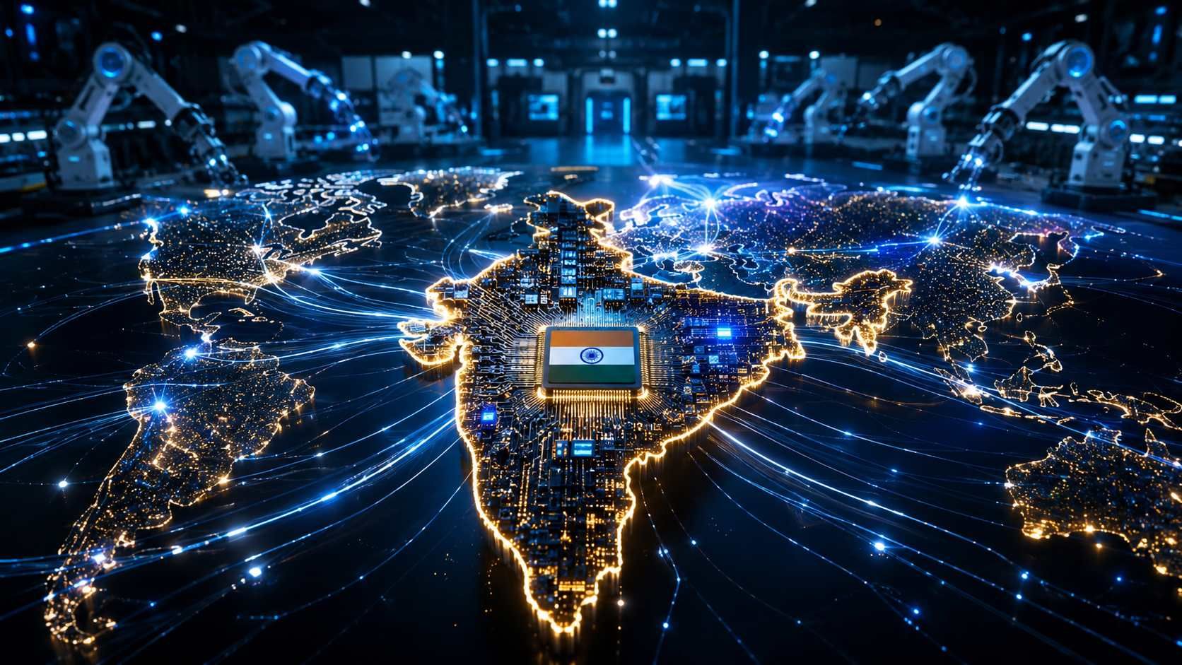
Global Semiconductor Sovereignty: An Exhaustive Analysis of India's Ascension as the Premier Silicon and AI Hub by 2030
When we look at the intricate web of the global macroeconomic and technological landscape as of May 2026, it becomes unequivocally clear that the worldwide semiconductor supply chain is undergoing a historic, irreversible geopolitical realignment. For several decades, the global production of integrated circuits, advanced memory packages, and artificial intelligence (AI) compute architecture was dangerously concentrated in a fragile East Asian corridor. This hyper-concentration left global markets severely vulnerable to geopolitical shocks, pandemic-induced supply chain collapses, and localized natural disasters. However, an in-depth analysis of the macroeconomic data, foreign direct investment (FDI) inflows, and technological milestones reveals that the Republic of India has rapidly transitioned from being a peripheral consumer of digital technology to serving as the central, pivotal architect of the global semiconductor and AI ecosystem.
Our analysis indicates that this transformation is not a mere accident of shifting global trade winds, but rather the result of an unprecedented convergence of state-sponsored fiscal incentives, aggressive deep-tech strategic alliances, and the mobilization of a massive demographic dividend of highly skilled engineering talent. India's trajectory points firmly toward undisputed global leadership. The domestic Indian semiconductor market, which was valued at a baseline of $38 billion USD (around 3.1 lakh crore rupees) in 2023, is currently experiencing exponential growth propelled by the relentless digitization of automotive electronics, industrial automation, telecommunications, and hyper-scale data centers.
Current predictive models and industry projections indicate that this market will reach $100 billion to $120 billion USD (around 8.3 lakh crore to 10 lakh crore rupees) by 2030. Pushing the timeline further, our assessment shows the market soaring to $180.20 billion USD (around 14.9 lakh crore rupees) by 2034, representing a formidable Compound Annual Growth Rate (CAGR) of 11.95%. By the end of 2035, the market is projected to reach an astounding $300 billion USD (around 24.9 lakh crore rupees), fundamentally restructuring the composition of the nation's Gross Domestic Product (GDP).
This exhaustive research report dissects the multidimensional architecture of India's semiconductor and AI revolution up to May 24, 2026. By thoroughly examining the India Semiconductor Mission (ISM) policy framework, front-end fabrication milestones, back-end assembly and testing capabilities, indigenous intellectual property (IP) development, and expansive global partnerships, our analysis clearly demonstrates how India is securing the future of the global AI economy.
1. The Strategic Policy Blueprint: Evolution of the India Semiconductor Mission (ISM)
To fully comprehend the sheer scale and velocity of India's silicon revolution, one must first analyze the foundational policy architecture that catalyzed this explosive growth: the India Semiconductor Mission (ISM). Established in December 2021 under the Ministry of Electronics and Information Technology (MeitY), the initial phase of this program (ISM 1.0) mobilized $10 billion USD (around 76,000 crore rupees) in fiscal incentives. This framework offered up to 50% capital subsidies on a pari-passu basis to seed a domestic ecosystem consisting of silicon fabs, compound semiconductor units, and Outsourced Semiconductor Assembly and Test (OSAT) facilities.
When we evaluate the execution of ISM 1.0, the data reflects a decisive, aggressive shift from mere policy intent to rapid physical infrastructure development. As of May 2026, the Indian government has successfully approved 12 major projects under the ISM, alongside one critical facility under the parallel Scheme for Promotion of Manufacturing of Electronic Components and Semiconductors (SPECS). This brings the total to 13 operational or under-development mega-projects across the country, representing cumulative investments that exceed $20 billion USD (around 1.64 lakh crore rupees).
1.1 The Transition to ISM 2.0: Deepening the Ecosystem
Recognizing that global competitiveness in the semiconductor industry requires continuous capital infusion, ecosystem depth, and long-term structural resilience, the Union Budget 2026–27 marked a decisive moment for India's technology ambitions with the official announcement of India Semiconductor Mission 2.0. While the primary objective of ISM 1.0 was to attract large-scale anchor manufacturers to establish a beachhead in India, our analysis of ISM 2.0 reveals a strategic policy pivot toward achieving structural self-reliance across the entire value chain.
The modified programme allocates a dedicated budget of ₹1,000 crore (around $120 million USD) specifically for the 2026-27 fiscal year to deepen domestic capabilities. Concurrently, the broader Modified Programme for Development of Semiconductor and Display Manufacturing Ecosystem in India commands a massive total financial outlay of ₹8,000 crore (around $960 million USD) for the same year. This represents the largest single-year fiscal outlay since the programme's inception, signaling to the global market that India's commitment is permanent and expanding.
ISM 2.0 explicitly targets the localization of semiconductor capital equipment, ultra-pure chemical materials manufacturing, advanced design capabilities, and the generation of full-stack indigenous intellectual property (IP). This ensures that India does not merely assemble foreign components, but fundamentally owns the technology that powers them.
1.2 Recent Mega-Project Approvals: The May 2026 Expansion
The momentum of the ISM framework has accelerated notably in the first half of 2026. On May 5, 2026, the Union Cabinet, chaired by the Prime Minister, approved two highly specialized semiconductor projects to be established in the state of Gujarat. These two projects command a combined investment of approximately $475 million USD (around 3,936 crore rupees) and are projected to generate high-quality employment for over 2,230 skilled engineering professionals.
| Project Developer | Location | Estimated Investment | Technological Focus and Production Capacity |
|---|---|---|---|
| Crystal Matrix Limited (CML) | Dholera, Gujarat | ~$370 million USD (₹3,068 crore) | Establishment of India's first commercial Mini/Micro-LED display facility utilizing Gallium Nitride (GaN) compound semiconductor technology. The facility will also provide GaN foundry services, including epitaxy on 6-inch wafers. Annual target: 72,000 sq. meters of display panels and 24,000 RGB wafer sets. |
| Suchi Semicon Private Limited | Surat, Gujarat | ~$105 million USD (₹868 crore) | Development of an Outsourced Semiconductor Assembly and Test (OSAT) facility dedicated to manufacturing discrete semiconductors, lead frames, and wirebond packaging. Annual target: 1,033.20 million chips for power electronics, automotive, and industrial automation. |
Our analysis reveals that these recent approvals are highly strategic and targeted. Crystal Matrix's focus on Gallium Nitride (GaN) is particularly noteworthy. GaN is a wide-bandgap compound semiconductor that offers vastly superior electron mobility, breakdown voltage, and thermal management compared to traditional silicon. By mastering GaN technology, India is positioning itself to capture the high-margin, high-growth global markets of Extended Reality (XR) glasses, smartwatches, high-frequency telecommunications, and advanced automotive displays. Simultaneously, Suchi Semicon fortifies the critical supply chain for consumer appliance microcontrollers and power electronics, directly supporting the broader electronics manufacturing sector in India.
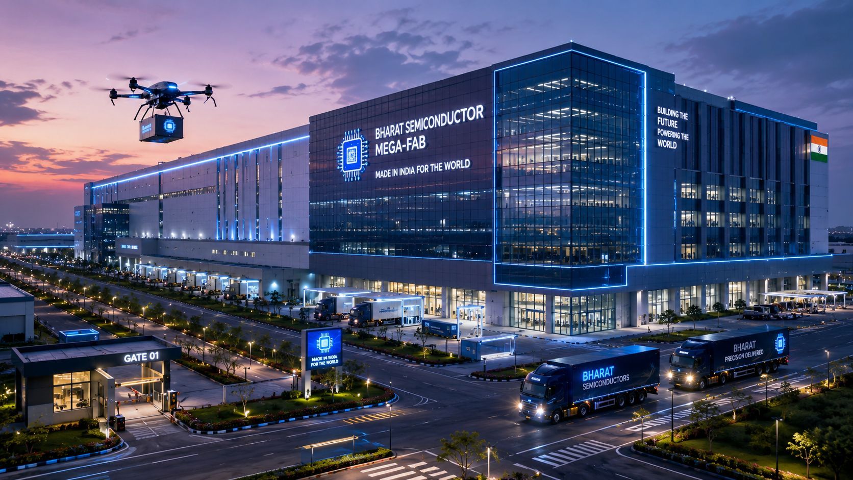
2. The Front-End Fabrication Revolution: The Dholera Mega-Fab Ecosystem
The crown jewel of India's semiconductor ascension is undoubtedly the successful establishment of commercial, high-volume front-end wafer fabrication facilities. For decades, the immense capital intensity, microscopic precision requirements, and staggering technical complexity of front-end fabs restricted their geographical footprint almost entirely to Taiwan, South Korea, and the United States. India has now forcefully and permanently shattered this barrier.
2.1 The Tata-PSMC Foundry Partnership
In a historic partnership with Taiwan's Powerchip Semiconductor Manufacturing Corporation (PSMC), Tata Electronics is currently developing India's first commercial 300-mm (12-inch) semiconductor fabrication plant in the Dholera Special Investment Region of Gujarat. Backed by an estimated investment of $11 billion USD (around 91,000 crore rupees), this mega-fab represents a paradigm shift in global supply chain diversification and economic sovereignty.
When we look at the technological roadmap of the Dholera fab, the strategy deployed by Tata and the Indian government is deliberately pragmatic, incremental, and highly effective. Rather than immediately engaging in the brutally capital-intensive, high-risk race for sub-3nm logic nodes (which are currently dominated by TSMC and Samsung), Tata and PSMC are initially focusing their manufacturing capabilities on mature and legacy nodes, specifically the 28nm, 40nm, 55nm, 90nm, and 110nm technology spectrums.
Our assessment indicates that this is a masterclass in global market entry. Mature nodes remain the undisputed, high-volume workhorses of the global digital economy. They are absolutely essential for automotive electronics (which require highly reliable, weather-resistant, and durable microcontrollers), mobile device power management integrated circuits (PMICs), Internet of Things (IoT) sensors, and heavy telecommunications infrastructure. By dominating the 28nm to 110nm spectrum, India is systematically insulating the global automotive and industrial sectors from future supply shocks, while simultaneously capturing massive market share in sectors where demand far outstrips global supply.
As of early 2026, the Dholera facility has reached a critical 50% construction milestone. The project has successfully navigated the grueling civil infrastructure development phase—which involves pouring massive concrete vibration-dampening foundations necessary for nanoscale lithography—and is now transitioning to the advanced technical setup, commonly known in the semiconductor industry as the "tool-in" phase. Trial production is firmly on schedule to commence by late 2026. To support the seamless operation of this massive industrial complex, the government officially notified Special Economic Zone (SEZ) status for the 66-hectare site on April 9, 2026, ensuring highly streamlined customs clearances, optimized logistics, and the integration of an on-site inland container depot.
2.2 The Historic ASML-Tata Catalyst: Securing the Silicon "Printing Press"
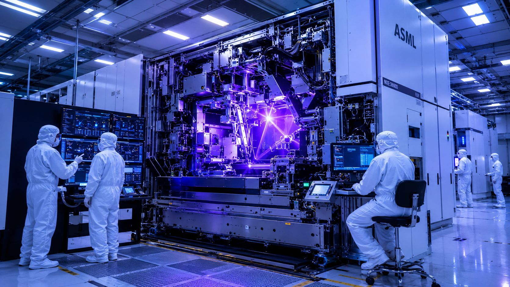
Perhaps the most profound and geopolitically significant development in India's semiconductor journey occurred recently on May 16, 2026. On this date, Tata Electronics and the Dutch semiconductor equipment manufacturing titan ASML signed a landmark strategic partnership agreement across The Hague, Netherlands, and Mumbai, India.
To grasp the true magnitude of this deal, one must understand the unique position ASML holds in the global economy. ASML possesses an absolute, unchallenged global monopoly on Extreme Ultraviolet (EUV) lithography machines, and is the undisputed world leader in Deep Ultraviolet (DUV) lithography. These machines utilize lasers, highly polished mirrors, and the principles of the Rayleigh criterion to print nanoscale circuit patterns onto silicon wafers. They are widely considered the most complex mechanical devices ever engineered by humanity, acting as the ultimate bottleneck in global chip production.
Under the umbrella of the Dholera fab's $11 billion USD (around 91,000 crore rupees) investment, ASML has committed to supplying a holistic suite of advanced lithography manufacturing technology and equipment to the Indian facility. However, an in-depth reading of the agreement parameters reveals that this is far more than a simple, transactional equipment sale. The partnership involves deep structural integration and capacity building, including:
- Talent and Skill Development: The partnership will focus on accelerating the intense training of local Indian engineers in lithography-specific skills. This effectively creates a domestic talent pipeline capable of operating, calibrating, and maintaining the world's most sophisticated optical machinery, ensuring long-term operational independence.
- R&D Infrastructure Integration: The two companies will cooperate to develop localized R&D infrastructure and domestic research initiatives. This is critical for pushing the boundaries of optical precision manufacturing, computational lithography, and defect reduction in Indian fabs.
- Supply Chain Resilience: Tata Electronics and ASML will work collaboratively to develop a proactive, highly resilient, and trusted supply chain matrix to protect the fab from global geopolitical disruptions and component shortages.
When evaluating global geopolitics, this alliance is nothing short of revolutionary. For ASML, transferring such sensitive technology to India provides a vital opportunity to diversify its geographic footprint away from its heavy, high-risk concentration in Taiwan, South Korea, and China. For India, possessing ASML lithography capability means the nation has officially acquired the foundational "printing press" of the digital era. This technological acquisition virtually guarantees India's future status as the next Taiwan in terms of manufacturing scale, precision engineering, and strategic global indispensability.
3. Advanced Packaging and OSAT: Securing the Critical Back-End
While front-end silicon fabrication rightfully commands global headlines due to its capital intensity, the realm of semiconductor packaging has evolved dramatically from a low-margin, labor-intensive afterthought into a highly critical technological frontier. With the physical limits of Moore's Law rapidly approaching, the global semiconductor industry is pivoting aggressively toward chiplets, heterogeneous integration, and advanced 2.5D/3D packaging. Our analysis shows that India is rapidly building formidable, world-class capacity in these exact domains.
3.1 The Micron Technology Benchmark in Sanand
India's back-end ecosystem achieved a historic, market-validating milestone on February 28, 2026, with the grand opening and operationalization of Micron Technology's state-of-the-art Assembly, Test, Marking, and Packaging (ATMP) facility in Sanand, Gujarat. Backed by an investment of $2.75 billion USD (around 22,800 crore rupees) jointly funded by Micron and government partners, this facility was inaugurated by Prime Minister Narendra Modi alongside Micron CEO Sanjay Mehrotra.
The Sanand facility converts advanced DRAM (Dynamic Random Access Memory) and NAND flash wafers from Micron's global manufacturing network into finished, globally distributed memory and storage products. It is crucial to note that the facility is not merely in a testing phase; it has secured the rigorous ISO 9001:2015 certification and officially commenced high-volume commercial production. During the inauguration, Micron presented its first shipment of globally integrated, "Made-in-India" high-end memory chips.
At over 500,000 square feet of highly controlled cleanroom space, the first phase of Micron's Sanand operation ranks among the world's largest single-floor assembly and test cleanrooms. It was designed explicitly to meet the surging, insatiable global demand for memory bandwidth fueled by the ongoing AI revolution.
3.2 Expanding and Decentralizing the OSAT Footprint
Beyond the anchor investment by Micron, India's OSAT ecosystem is deliberately decentralizing, creating highly specialized technological hubs across multiple states to mitigate geographic risk. When we look at the broader map of India's back-end infrastructure, a massive, interconnected network of facilities emerges:
| Company / Joint Venture | Location | Estimated Investment | Technological Focus |
|---|---|---|---|
| CG Semi Private Limited (CG Power & Renesas) | Sanand, Gujarat | ~$915 million USD (₹7,600 crore) | Launched in August 2025, this is India's first full-service OSAT provider offering both traditional wirebond and highly advanced packaging technologies for industrial and automotive applications. |
| HCL Group & Foxconn JV | Jewar, Uttar Pradesh | ~$389.9 million USD (₹3,706 crore) | An OSAT facility focused on manufacturing display driver integrated circuits (ICs) used in smartphones, laptops, PCs, and automotive systems. Taiwan's CTCI Corporation is serving as the engineering and procurement partner. |
| 3D Glass Solutions Inc. (3DGS) | Bhubaneswar, Odisha | ~$234 million USD (₹1,943 crore) | A cutting-edge facility producing glass panel substrates and ATMP services. Target output includes 69,600 glass panel substrates and 13,200 3DHI modules annually for high-performance computing, RF, and defense applications. |
| Tata Semiconductor Assembly and Test (TSAT) | Jagiroad, Assam | ~$3.2 billion USD (₹27,000 crore) | A massive greenfield ATMP facility focusing on multiple packaging technologies, including traditional, advanced, and wafer platforms, expanding the ecosystem into Northeast India. |
| Kaynes Semicon | Sanand, Gujarat | ~$397 million USD (₹3,300 crore) | Secured OSAT project approvals to contribute to India's semiconductor packaging and testing capabilities, adding crucial volume to the Gujarat cluster. |
The inclusion of 3D Glass Solutions (3DGS) in Odisha is particularly indicative of India's forward-looking strategy. As the industry moves beyond organic substrates, glass substrates are universally recognized as the future of advanced packaging due to their superior thermal stability and interconnect density. By establishing this facility, India is leapfrogging legacy technologies and embedding itself in the next generation of computing architecture.
3.3 The Return of Tower Semiconductor: Targeting the Analog Market
Further illustrating the immense momentum in the manufacturing sector, Israel-based Tower Semiconductor—widely recognized as one of the world's leading pure-play analog semiconductor foundries—has submitted a comprehensive $8 billion to $10 billion USD (around 66,000 crore to 83,000 crore rupees) proposal to establish a semiconductor fab in Taloja, Panvel, near Mumbai, Maharashtra. This proposal is in partnership with the Indian conglomerate Adani Group.
Following the collapse of Intel's attempted $5.4 billion USD acquisition of Tower (which failed due to a lack of regulatory approval from Chinese authorities), the Israeli firm has strategically re-focused its global expansion efforts on the secure, democratic Indian market. The proposed Maharashtra facility intends to manufacture 65nm and 40nm chips.
Our analysis indicates that this development is of paramount importance because analog and mixed-signal semiconductors—which include radio frequency (RF) chips, silicon photonics, power management ICs, and sensor interfaces—are absolutely indispensable for the operation of 5G communications, aerospace arrays, defense radars, medical imaging, and electric vehicles. The successful realization of this joint venture will not only add massive scale to India's capacity but will further cement the nation's total dominance over the mature node and analog global markets.
4. Artificial Intelligence Compute: Bridging the Hardware Deficit

The technological convergence of advanced semiconductors and Artificial Intelligence represents the absolute apex of modern geoeconomic power. Official estimates project that the integration of AI could inject a staggering $1.7 trillion USD (around 141 lakh crore rupees) into India's GDP by 2035. Furthermore, industry surveys reveal that nearly 87% of Indian enterprises are already leveraging some form of AI in their daily operations. However, the global AI landscape is currently defined by a harsh, restrictive reality: raw compute capacity is the new strategic national infrastructure, and the global supply of advanced AI Graphics Processing Units (GPUs) is heavily monopolized.
4.1 The Geopolitics of the GPU Chokepoint
An in-depth look at global AI compute hardware reveals a vast and dangerous imbalance. As of 2025 and early 2026, the United States effectively controls approximately 75% of the world's AI compute capacity. This dominance is driven by American hyperscalers like Microsoft, Google, and Amazon, which routinely deploy massive server clusters containing upwards of 100,000 GPUs for individual data centers.
The financial barrier to entry is immense; a single cutting-edge Nvidia Blackwell GPU commands a price tag ranging from $40,000 to $45,000 USD (around 33 lakh to 37 lakh rupees). Furthermore, the United States government utilizes a tiered export control regime to dictate international hardware allocation, placing strict caps on the dissemination of these chips to ensure American geopolitical dominance.
Compounding this geopolitical risk is the physical manufacturing chokepoint. While Nvidia designs these chips, they do not manufacture them. Over 90% of the world's advanced logic chips—including essentially all Nvidia GPUs, Apple processors, and advanced AMD chips—are manufactured by TSMC on the island of Taiwan. This represents a severe, unacceptable geostrategic vulnerability for any nation attempting to build an independent AI ecosystem.
4.2 The IndiaAI Mission: Democratizing Compute Capacity
To ensure that India does not remain a mere consumer of AI technologies built, regulated, and censored elsewhere, the Indian government has aggressively scaled the scope of the IndiaAI Mission. The mission's core objective is to democratize access to cutting-edge AI hardware for domestic startups, academic researchers, and industry innovators, effectively preventing an "innovation drain" to Western cloud providers.
Backed by a massive budgetary outlay of ₹10,372 crore (around $1.25 billion USD), the IndiaAI Mission has significantly expanded its initial deployment targets. By late 2025 and early 2026, the government successfully completed the empanelment and deployment of over 18,000+ top-tier AI compute units (GPUs and AI accelerators), far exceeding their original planning parameters.
The technological diversity of this hardware empanelment is highly strategic. Following rigorous evaluation, ten agencies were selected to provide cloud-based AI compute services featuring a diversified, vendor-agnostic portfolio of processors. This includes:
- Nvidia Architecture: H100, H200, and A100 Tensor Core GPUs.
- AMD Architecture: Instinct MI300X Accelerators.
- Intel Architecture: Gaudi 2 AI Accelerators.
- Cloud-Native Architecture: AWS Trainium instances.
Crucially, under the IndiaAI Mission, the government heavily subsidizes the cost of this computing power, making it available to eligible domestic users at up to a 40% reduced cost compared to global market rates. When we evaluate this strategy, it becomes abundantly clear that India is methodically building a robust, sovereign AI training infrastructure. This infrastructure completely insulates domestic deep-tech ecosystems from volatile global pricing models and the constant threat of foreign export control shocks, allowing Indian AI models to be trained on Indian data, using Indian-controlled compute.

5. Indigenous Intellectual Property: The Design-Led Revolution
While manufacturing physical hardware is vital for supply chain security, the highest economic value capture within the semiconductor ecosystem lies in architecture, logic design, and intellectual property (IP) creation. India is currently leveraging its massive historical advantage—possessing nearly 20% of the entire global semiconductor design workforce—to permanently transition from providing back-office engineering support to driving front-end indigenous innovation.
5.1 The 3-Nanometer Innovation Frontier
On May 13, 2025, Union Minister Ashwini Vaishnaw unveiled a monumental technological achievement: the official inauguration of India's first 3-nanometer (3nm) chip design centers, located in the tech hubs of Noida and Bengaluru. Operated in close collaboration with the Japanese semiconductor titan Renesas Electronics, these cutting-edge facilities mark India's definitive entry into the most elite, exclusive echelon of global semiconductor innovation.
Designing silicon at the 3nm node is an exercise in extreme physics. It requires complete mastery over quantum tunneling effects, extreme thermal dynamics, and the utilization of highly advanced Electronic Design Automation (EDA) tools. The successful establishment of these centers signifies to the global market that Indian engineers are no longer just updating and maintaining legacy systems; they are actively architecting the quantum-scale brains of tomorrow's AI server farms, autonomous vehicles, and next-generation defense systems.
5.2 Dhruv64 and the RISC-V Open Architecture Movement
The most compelling, undeniable evidence of India's aggressive drive toward total silicon sovereignty is the successful development and commercial launch of the Dhruv64 microprocessor. Developed fully indigenously by the Centre for Development of Advanced Computing (C-DAC) under the Microprocessor Development Programme (MDP) and the Digital India RISC-V (DIR-V) initiative, Dhruv64 is an absolute masterstroke in hardware independence.
When we look at the technical specifications of Dhruv64, its capability is highly impressive for a fully indigenous project:
- Architecture: It is a 64-bit dual-core processor utilizing the open-source RV64G (IMAFD) instruction set.
- Performance: Features a robust clock speed of 1.0 GHz.
- Manufacturing: Fabricated on a 28nm process node, comprising approximately 30 million logic gates.
- Target Application: Designed as an application-class processor tailored specifically for industrial automation, robotics, secure telecommunications, and robust infrastructure segments.
When evaluating the strategic significance of Dhruv64, the underlying architecture is the critical factor. By utilizing the open-source RISC-V instruction set architecture, the Indian government completely circumvents the exorbitant licensing fees, restrictive usage terms, and severe geopolitical chokepoints associated with proprietary, Western-controlled architectures like ARM (UK/US) and x86 (Intel/AMD).
Dhruv64 joins a rapidly expanding family of highly specialized, homegrown Indian silicon. This includes SHAKTI (developed by IIT Madras for strategic, space, and defense applications), AJIT (developed by IIT Bombay for robotics), VIKRAM (developed by ISRO for withstanding the extreme radiation of space conditions), and the THEJAS32/64 series.
Our analysis reveals that the rapid proliferation of these indigenous chips, heavily supported by the government's Design Linked Incentive (DLI) scheme, ensures a secure future. It guarantees that India's military hardware, space command infrastructure, and critical civilian networks (such as power grids and telecom switches) will soon operate entirely on trusted, hack-proof, indigenous silicon architecture. Furthermore, the next-generation System on a Chip (SoC) designs, named DHANUSH and DHANUSH+, are already in the advanced development phase, promising to push performance metrics even further into the gigahertz spectrum.
6. Upstream Localization: Securing the Chemical, Material, and Equipment Supply Chain
A holistic assessment of the global semiconductor supply chain highlights a historical, critical vulnerability for India: an over 90% dependence on imported foundational upstream inputs. These inputs include highly purified photoresists, specialized etching gases, raw silicon wafers, chemical mechanical polishing (CMP) slurries, and ultra-pure water. Without domesticating the production of these foundational materials, the multi-billion-dollar downstream fabs being built in Gujarat and Assam remain critically exposed to geopolitical supply shocks and international logistics failures.
Recognizing this existential risk, the ISM 2.0 policy framework aggressively targets the domestication of the chemical and capital equipment sectors. This targeted policy approach has successfully attracted the premier titans of global semiconductor equipment manufacturing to set up physical roots in India.
6.1 Anchoring Lam Research and Applied Materials
American semiconductor equipment giant Lam Research has officially committed to an investment exceeding $1 billion USD (around 8,300 crore rupees) in the state of Karnataka. This massive capital injection is designed to bolster semiconductor tool engineering, advance process technology, and fund massive ecosystem training programs. Formalized through a strategic Memorandum of Understanding with the Karnataka Industrial Area Development Board, this investment secures the localized engineering, production support, and maintenance of the highly complex plasma etching and deposition tools that are vital for advanced chip manufacturing.
Simultaneously, Applied Materials, another heavyweight in the capital equipment sector, has invested heavily in the region, announcing a $400 million USD (around 3,300 crore rupees) collaborative engineering center in Bangalore. This sprawling center brings together Applied's elite engineers, domestic Indian suppliers, and leading academic institutions to accelerate the R&D and commercialization of semiconductor equipment sub-systems. By establishing this global innovation infrastructure on Indian soil, the nation is steadily and methodically weaning itself off its historical reliance on foreign-assembled capital equipment.
To support this massive influx, state-level policies are adapting rapidly. The Karnataka state government, during its 2026-27 Budget presentation, announced that it anticipates total investments to the tune of ₹45,000 crore (around $5.4 billion USD) specifically within the semiconductor and electronics sector. To absorb this, the state is expanding its infrastructure, including the establishment of a dedicated robotics and artificial intelligence campus under the AI and Robotics Technology Park at the Indian Institute of Science.
6.2 The Japanese Materials Corridor: A Strategic Synergy
To bridge the highly specialized chemical and materials deficit, India has actively and successfully courted the Japanese industrial base. Historically, Japan holds a virtual global stranglehold on the production of specialty semiconductor chemicals and ultra-pure materials. A highly significant Track 1.5 conference held in New Delhi, followed by a detailed report published in March 2026, formalized this strategic convergence.
The underlying logic of this bilateral relationship is flawless: Japan possesses world-class specialty chemical producers, advanced materials expertise, and equipment firms, but lacks domestic growth. India offers massive, immediate domestic demand, a sprawling design workforce, and an aggressive policy architecture offering deep subsidies.
This synergy is already materializing through high-level joint ventures and the formal India-Japan Semiconductor Policy Dialogue. These institutional frameworks are actively facilitating the localization of wafer precursors, encapsulation resins, and high-grade etching gases directly within India. This effectively builds a robust, self-sustaining micro-economy of suppliers clustered immediately around the mega-fabs in Gujarat, Uttar Pradesh, and Assam.
7. Global Geopolitics, International Partnerships, and the "China+1" Realization
India's meteoric success in the semiconductor domain is not occurring in a vacuum; it is the deliberate, calculated result of supreme geopolitical maneuvering on the world stage. As the United States, the European Union, and their allied nations actively seek to decouple their critical supply chains from Chinese technology ecosystems (a macroeconomic movement known universally as the "China+1" strategy), they simultaneously seek to mitigate the catastrophic risk of a potential cross-strait military conflict in Taiwan. In this volatile environment, India has perfectly positioned itself as the only democratic nation possessing the necessary geographical scale, political stability, and deep engineering talent pool to serve as the ultimate global counterweight.
7.1 Strategic Bilateral and Multilateral Pacts
The alignment of global tech security is evidenced by an intricate, binding web of bilateral agreements formulated between 2023 and 2026:
- United States - Japan Technology Prosperity Deal (Oct 2025): While this is technically a bilateral agreement between Washington and Tokyo to usher in a "Golden Age of Innovation" via AI and quantum technology, the pact explicitly recognizes the critical importance of deepening science and tech ties with strategic partners across the broader Indo-Pacific. Our analysis views this as the formal setting of the stage for the seamless transfer of technology and the integration of Indian fabs directly into the ultra-secure US-Japan defense and AI supply chains.
- EU-India Semiconductor Agreement: Operationalized heavily through the EU-India Trade and Technology Council (TTC), the European Union and India are collaborating intensely to ensure global supply chains that can easily withstand global disruptions. The EU's official proposal to create "Blue Valleys"—dedicated geographic platforms designed to accelerate private-sector engagement, standard alignment, and deep skill development—demonstrates Europe's absolute reliance on India for its long-term technological security and green energy transition.
- The Taiwan Dividend: When the United States and Taiwan entered into a massive $250 billion USD (around 20.7 lakh crore rupees) direct investment and trade deal in January 2026 to secure American domestic supply chains, the geopolitical spillover effect was immediate. Recognizing that their domestic capacity was maxed out and geographically vulnerable, Taiwanese tech giants rapidly expanded their Indian footprints to maintain global market share. PSMC's willingness to engage in deep technology transfer to Tata Electronics is a direct, tangible result of Taiwan aggressively seeking geostrategic redundancy through Indian scale.
7.2 Corporate Alliances: The Tata Group's Global Footprint
To truly appreciate the depth of India's integration into the global technology nervous system, one must examine the staggering corporate alliances forged by the Tata Group—the undisputed vanguard of India's tech renaissance:
- Tata and Intel Strategic Alliance (December 2025): In a move that sent shockwaves through the industry, the Tata Group entered into a strategic alliance with Intel Corporation, an agreement reportedly valued by market analysts at over $14 billion USD (around 1.16 lakh crore rupees) in synergistic potential. This massive collaboration focuses on exploring the manufacturing and advanced packaging of Intel products for local markets at Tata's facilities. More importantly, it aims to rapidly scale tailored AI PC solutions, leveraging Intel's AI compute reference designs alongside Tata's vast Electronics Manufacturing Services (EMS) capabilities. This alliance fundamentally ties the legacy American chipmaker's future growth directly to India's domestic manufacturing capability.
- Tata and Qualcomm Partnership (February 2026): Tata established a sweeping, comprehensive partnership to manufacture Qualcomm Automotive Modules directly at Tata's OSAT facility in Assam. This agreement guarantees that global automakers who rely on Qualcomm's advanced Snapdragon Digital Chassis for their next-generation vehicles will now be sourcing their critical electronic components directly from Indian fabs. This action irrevocably integrates India deeply into the core of the global automotive supply chain.
- Tata and ROHM Partnership (December 2025): Partnering with the leading Japanese semiconductor manufacturer ROHM Co., Ltd., Tata aims to drastically expand the lineup of domestically produced, high-efficiency packaged semiconductor products. This ensures that products jointly manufactured in India will be supplied directly to the global market, helping to build a sustainable, region-based supply chain network.
Our analysis confirms that these high-level alliances represent a structural, permanent locking-in of global tech giants into the Indian ecosystem. It is no longer a matter of India attempting to attract foreign companies with subsidies; global technology leadership is now heavily, structurally dependent on Indian execution and manufacturing scale.
8. Market Forecast and The Economic Transformation

The synthesis of these highly localized policy initiatives, massive infrastructure buildouts, and deep global partnerships translates into staggering macroeconomic forecasts. The transformation of India from an emerging market to a pivotal, central geoeconomic anchor is irrefutable and backed by hard data.
8.1 The Exponential Growth Trajectory
As previously noted, the domestic Indian semiconductor market was valued at approximately $38 billion USD (around 3.1 lakh crore rupees) in 2023, meeting its demand almost entirely through foreign imports. Driven by the explosive, nationwide adoption of Artificial Intelligence, the rapid penetration of electric vehicles (EVs), the rollout of 5G/6G telecommunications infrastructure, and hyper-scale data center expansion, current expert consensus places the market size in the $45 billion to $50 billion USD (around 3.7 lakh crore to 4.1 lakh crore rupees) range for the 2024-2025 financial period.
Looking forward, the growth curve steepens dramatically. Forecasts project the market will command a valuation of $100 billion to $120 billion USD (around 8.3 lakh crore to 10 lakh crore rupees) by 2030, eventually reaching $180.20 billion USD (around 14.9 lakh crore rupees) by 2034. Leading analytical models from global consultancy firms suggest that by the end of 2035, the market could triple to an astounding $300 billion USD (around 24.9 lakh crore rupees). This growth trajectory will fundamentally restructure India's economic output, moving it decisively away from traditional IT services and toward high-value, deep-tech hardware manufacturing.
8.2 Reversing the Trade Deficit and Achieving Sovereignty
Historically, India suffered from a severe technological trade deficit, importing over 90% of its total semiconductor and electronic component requirements. However, the data resulting from the ISM implementations projects a massive, historic structural shift. By 2030, India officially targets a 20% domestic supply sufficiency rate, and by 2035, local production from facilities like Dholera and Sanand is expected to meet more than 60% of total domestic demand.
When we evaluate this from a macroeconomic perspective, this transition represents one of the most significant and rapid import substitution events in modern global economic history. Not only will this save the nation tens of billions of dollars in foreign exchange reserves annually, but it simultaneously establishes India as a net exporter of highly critical technology. India is on the definitive path to becoming the world's primary supplier of mature node logic chips, advanced heterogeneous memory packages, and highly durable automotive microcontrollers.

9. Conclusion: The Irreversible Trajectory of Leadership
When evaluating the comprehensive, global landscape of the semiconductor and artificial intelligence industry in May 2026, the accumulated evidence points to a definitive, undeniable conclusion: India's metamorphosis into a top-tier semiconductor and AI leader is no longer a speculative projection, a hopeful policy paper, or a distant ambition. It is an unfolding, highly capitalized physical reality.
Through the brilliantly structured, heavily funded, and multi-phase India Semiconductor Mission (ISM 1.0 and 2.0), the government has successfully converted massive fiscal outlays into tangible steel, pouring concrete, and operational nanoscale cleanrooms. By securing the historic, multi-billion-dollar ASML lithography partnership, India has permanently broken the historic technological monopoly previously held by the East Asian corridor, assuring its long-term place as a front-end foundry powerhouse capable of independent innovation. Simultaneously, the rapid, flawless operationalization of mega ATMP and OSAT facilities by global giants like Micron, CG Power, and the HCL-Foxconn joint venture has thoroughly solidified the back-end supply chain, ensuring that chips manufactured in India are packaged and shipped from India.
Moreover, India has masterfully navigated the highly restrictive, geopolitically fraught chokepoints of the Artificial Intelligence revolution. By heavily subsidizing high-end GPU compute access for domestic startups through the billion-dollar IndiaAI Mission, while concurrently engineering the open-source, fully indigenous Dhruv64 RISC-V architecture, the nation has achieved a highly sophisticated, enviable balance. It has perfectly merged the benefits of cutting-edge global integration with the absolute security of resilient technological sovereignty.
The current geopolitical convergence of American capital equipment (Lam Research, Applied Materials), Dutch extreme lithography (ASML), Japanese ultra-pure materials (Rohm, Renesas), Taiwanese operational and manufacturing expertise (PSMC, Foxconn), and Indian scale, policy support, and engineering talent has birthed an unstoppable technological ecosystem. As the global economy transitions deeper into the AI-driven Silicon Age, the Republic of India stands unassailable—not merely as a willing participant or an alternative manufacturing hub, but as the premier architect, the primary engine of growth, and the most trusted custodian of the global technological future.
Related Topics:
"Tracking the carbon economy, decoding global climate treaties, and analyzing the massive environmental forces reshaping human civilization and global industry."
"Decoding the rapid evolution of artificial intelligence, deep-space breakthroughs, and the critical frontier of human science and bio-tech."
"Decoding the rapid evolution of artificial intelligence, deep-space breakthroughs, and the critical frontier of human science and bio-tech."
"Decoding the high-stakes chess game of global statecraft, strategic diplomacy, and the shifting balance of world power."
"Curating the elite intersection of global culture, cinematic intelligence, high-end gastronomy, and the premium evolution of modern lifestyle."

WPP Frontier Labs
Decoding the rapid evolution of artificial intelligence, deep-space breakthroughs, and the critical frontier of human science and bio-tech.
Get the Weekend Intelligence Briefing
Sign up for the deepest geopolitical and tech insights sent directly to your inbox every Sunday.
No spam. Unsubscribe anytime. View our Privacy Policy.